Features: ` On-Resistance, <400 max
` Transition Time, <500ns
` On-Resistance Match, <10
` NO-Off Leakage Current, <20pA at +25°C
` 1.5pC Charge Injection
` Single-Supply Operation (+4.5V to +30V)
Bipolar-Supply Operation (±4.5V to ±20V)
` Plug-In Upgrade for Industry-Standard
DG508A/DG509A
` Rail-to-Rail Signal Handling
` TTL/CMOS-Logic Compatible
` ESD Protection >2000V, per Method 3015.7Application·Data-Acquisition Systems
·Sample-and-Hold Circuits
·Test Equipment
·Heads-Up Displays
·Military Radios
·Communications Systems
·Guidance and Control Systems
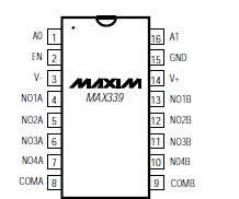
·PBX, PABXPinout
SpecificationsVoltage Referenced to
VV+..........................................................................-0.3V, 44V
GND.........................................................................-0.3V, 25V
Digital Inputs, NO, COM (Note 1)...........(V- - 2V) to (V+ + 2V) or
30mA (whichever occurs first)
Continuous Current (any terminal) ....................................30mA
Peak Current, NO or COM
(pulsed at 1ms, 10% duty cycle max) ..........................100mA
Continuous Power Dissipation (TA = +70°C)
Plastic DIP (derate 10.53mW/°C above +70°C) ........842mW
Narrow SO (derate 8.70mW/°C above +70°C) ..........696mW
CERDIP (derate 10.00mW/°C above +70°C)..............800mW
Operating Temperature Ranges
MAX33_C__ .......................................................0°C to +70°C
MAX33_E__.....................................................-40°C to +85°C
MAX33_MJE ..................................................-55°C to +125°C
Storage Temperature Range ...........................-65°C to +150°C
Lead Temperature (soldering, 10sec) .............................+300°C
Note 1: Signals on NO, COM, EN, A0, A1, or A2 exceeding V+ or V- are clamped by internal diodes. Limit forward current to maximum current ratings.
Stresses beyond those listed under "Absolute Maximum Ratings" may cause permanent damage to the device. These are stress ratings only, and functional operation of the device at these or any other conditions beyond those indicated in the operational sections of the specifications is not implied. Exposure to absolute maximum rating conditions for extended periods may affect device reliability.
DescriptionThe MAX338/MAX339 are monolithic, CMOS analog multiplexers (muxes). The 8-channel MAX338 is designed to connect one of eight inputs to a common output by control of a 3-bit binary address. The dual, 4-channel MAX339 is designed to connect one of four inputs to a common output by control of a 2-bit binary address. Both devices can be used as either a mux or a demux. On-resistance is 400 max, and the devices conduct current equally well in both directions.
These muxes feature extremely low off leakages (less than 20pA at +25°C), and extremely low on-channel leakages (less than 50pA at +25°C). The new design offers guaranteed low charge injection (1.5pC typ) and electrostatic discharge (ESD) protection greater than 2000V, per method 3015.7. These improved muxes are pin-compatible upgrades for the industry-standard DG508A and DG509A. For similar Maxim devices with lower leakage and charge injection but higher on-resistance,see the MAX328 and MAX329.
The MAX338/MAX339 operate from a single +4.5V to +30V supply or from dual supplies of ±4.5V to ±20V.All control inputs (whether address or enable) are TTL compatible (+0.8V to +2.4V) over the full specified temperature range and over the ±4.5V to ±18V supply range. These parts are fabricated with Maxim's 44V silicon-gate process.

 MAX339 Data Sheet


