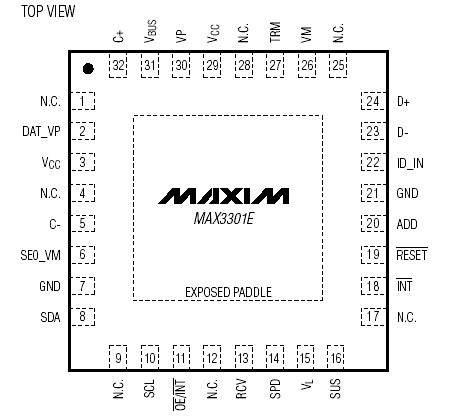
Features: ·USB 2.0-Compliant Full-/Low-Speed OTG Transceivers
·Ideal for USB On-the-Go, Embedded Host, or Peripheral Devices
·±15kV ESD Protection on ID_IN, VBUS, D+, and DTerminals
·Charge Pumps for VBUS Signaling and Operation Down to 3V
·Internal VBUS and ID Comparators
·Internal Switchable Pullup and Pulldown Resistors for Host/Peripheral Functionality
·I2C Bus Interface with Command and Status Registers
·Linear Regulator Powers Internal Circuitry and D+/D- Pullup Resistors
·Supports Car Kit Interrupts and Audio-Mode Operation
·Supports SRP and HNP
·Low-Power Shutdown Mode
·Available in 32-Pin Thin QFN and 5 x 5 UCSP Packages
Application·Mobile Phones
·PDAs
·Digital Cameras
·MP3 Players
·Photo PrintersPinout SpecificationsAll voltages are referenced to GND.
VCC, VL ......................................................................-0.3V to +6V
TRM (regulator off or supplied by VBUS) ....-0.3V to (VBUS + 0.3V)
TRM (regulator supplied by VCC)..................-0.3V to (VCC + 0.3V)
D+, D- (transmitter tri-stated) ..................................-0.3V to +6V
D+, D- (transmitter functional).....................-0.3V to (VCC + 0.3V)
VBUS .........................................................................-0.3V to +6V
ID_IN, SCL, SDA.........................................................-0.3V to +6V
INT , SPD, RESET, ADD, OE/INT, RCV, VP,
VM, SUS, DAT_VP, SE0_VM ..............................-0.3V to (VL + 0.3V)
C+...............................................................-0.3V to (VBUS + 0.3V)
C-..................................................................-0.3V to (VCC + 0.3V)
Short-Circuit Duration, VBUS to GND ............................Continuous
Continuous Power Dissipation (TA = +70)
5 x 5 UCSP (derate 12.2mW/°C above +70) ..................976mW
32-Pin Thin QFN (5mm x 5mm x 0.8mm) (derate 21.3mW/
above +70).....................................................................1702mW
Operating Temperature Range .................................-40 to +85
Junction Temperature...........................................................+150
Storage Temperature Range ..................................-65 to +150
Lead Temperature (soldering, 10s) ......................................+300
Bump Reflow Temperature (Note 1)
Infrared (15s) .......................................................................+200
Vapor Phase (20s) .................................................................+215DescriptionThe MAX3301E fully integrated USB On-the-Go (OTG) transceiver and charge pump allows mobile devices such as PDAs, cellular phones, and digital cameras to interface directly with USB peripherals and each other without the need of a host PC. Use the MAX3301E with an embedded USB host to directly connect to peripherals such as printers or external hard drives.
The MAX3301E integrates a USB OTG transceiver, a VBUS charge pump, a linear regulator, and an I2C™- compatible, 2-wire serial interface. An internal level shifter allows the MAX3301E to interface with logic supply voltages from +1.65V to +3.6V. The MAX3301E's OTG-compliant charge pump operates with +3V to +4.5V input supply voltages, and supplies an OTG-compatible output on VBUS while sourcing more than 8mA of output current.
The MAX3301E enables USB OTG communication from highly integrated digital devices that cannot supply or tolerate the +5V VBUS levels that USB OTG requires. The device supports USB OTG session-request protocol (SRP) and host-negotiation protocol (HNP) by controlling and measuring VBUS using internal comparators.
The MAX3301E provides built-in ±15kV electrostaticdischarge (ESD) protection for the VBUS, ID_IN, D+, and D- terminals. The MAX3301E is available in 5 x 5 chip-scale (UCSP™) and 32-pin (5mm x 5mm x 0.8mm) thin QFN packages and operates over the extended -40 to +85 temperature range.

 MAX3301E Data Sheet


