Features: Wide Operating Frequency Range
800MHz to 1000MHz (MAX2651/52)
1800MHz to 2000MHz (MAX2651/52/53)
Excellent Low-Noise Performance
1.2dB/1.3dB over GSM Receive Band (MAX2651/52)
1.8dB/1.8dB/1.7dB over DCS Receive Band (MAX2651/52/53)
High Gain
18dB over GSM Receive Band (MAX2651/52)
18dB/17.5dB/18.5dB over DCS Receive Band (MAX2651/52/53)
20dB Gain Reduction in Low-Gain Mode
Externally Adjustable Gain
+2.7V to +3.3V Single-Supply Operation
Low Supply Current
5.4mA to 7.0mA in High-Gain Mode
2.2mA in Low-Gain Mode
0.25µA Shutdown Current (MAX2652/53)ApplicationGSM900/DCS1800 Dual-Band Phones
GSM900/DCS1800/PCS1900 Triple-Band Phones
DCS1800 or PCS1900 Single-Mode Phones
IS-136 TDMA Dual-Band PhonesPinout Specifications
VCC to GND..........................................................-0.3V to +6V
SHDN, GAIN, BAND to GND......................-0.3V to (VCC + 0.3V)
GSMIN, DCSIN .........................................1.0V peak (+10dBm)
Input Current (all digital inputs) ..................................±10mA
Continuous Power Dissipation
8-Pin µMAX (derate 4.5mW/°C above +70°C)............362mW
10-Pin µMAX (derate 5.6mW/°C above +70°C) .........444mW
Operating Temperature Range .....................-40°C to +85°C
Junction Temperature..................................................+150°C
Storage Temperature Range .......................-65°C to +150°C
Lead Temperature (soldering, 10sec) .........................+300°C
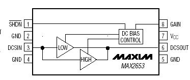
DescriptionThe MAX2651/MAX2652/MAX2653 silicon germanium (SiGe), low-noise amplifiers (LNAs) are intended for use in GSM900, DCS1800, and PCS1900 band wireless handsets. The MAX2651/MAX2652 consist of two LNAs, one optimized for the GSM900 band and the other optimized for the DCS1800/PCS1900 bands. They feature a band-select pin to switch between the two LNAs, as well as a gain-step input to reduce the gain of each LNA by 20dB and reduce supply current. The MAX2652 is functionally equivalent to the MAX2651, but features a lowpower shutdown mode. The MAX2653 consists of a single LNA optimized for the DCS1800 and PCS1900 bands, and has a shutdown feature and a 20dB gain step.
The MAX2652 and MAX2653 together form an ideal solution for triple-band phone applications (GSM, DCS, and PCS bands).
The MAX2651/MAX2652/MAX2653 are fabricated using an advanced high-frequency SiGe bipolar process. As a result, all devices provide low noise figure, high gain, and high input third-order intercept point (IP3) performance at the GSM, DCS, and PCS bands. A pull-up resistor to VCC at each LNA output allows for gain adjustability. A minimal umber of external components are needed for input and output matching, helping to reduce board space.
The MAX2651/MAX2652 are packaged in a 10-pin µMAX, while the MAX2653 is packaged in an 8-pin µMAX. All devices operate from a single +2.7V to +3.3V supply.

 MAX2653 Data Sheet


