Features: ` Single +2.7V to +5.5V Supply
` Complete Receive Path: 200MHz to 440MHz (first IF) to 8MHz to 13MHz (second IF)
` Limiter with Differential Outputs (adjustable level)
` RSSI Function with 90dB Monotonic Dynamic Range
` Complete Transmit Path: 8MHz to 13MHz (second IF) to 200MHz to 440MHz (first IF)
` On-Chip Oscillator with Voltage Regulator and Buffer
` Advanced System Power Management (four modes)
` 0.1A Shutdown Supply CurrentApplication ·PWT1900 Wireless Handsets and
·Base Stations
·PACS, PHS, DECT and Other PCS
·Wireless Handsets and Base Stations
·400MHz ISM Transceivers
·IF Transceivers
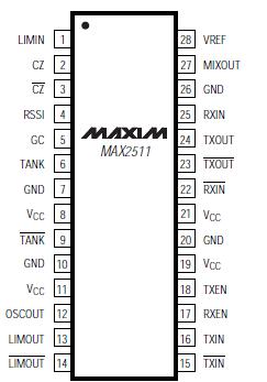
·Wireless Data LinksPinout Specifications
VCC to GND .............................................................-0.3V to 8.0V
VCC to Any Other VCC ........................................................±0.3V
TXIN, TXIN Input Voltage............................-0.3V to (VCC + 0.3V)
TXIN to TXIN Differential Voltage ...................................±300mV
RXIN, RXIN Input Voltage .......................................-0.3V to 1.6V
TANK, TANK Voltage................................................-0.3V to 2.0V
LIMIN Voltage ...............................(VREF - 1.3V) to (VREF + 1.3V)
LIMOUT, LIMOUT Voltage ................(VCC - 1.6V) to (VCC + 0.3V)
RXEN, TXEN, GC Voltage.............................-0.3V to (VCC + 0.3V)
RXEN, TXEN, GC Input Current ............................................1mA
RSSI Voltage.............................................-.0.3V to (VCC + 0.3V)
Continuous Power Dissipation (TA = +70°C)
QSOP (derate 11mW/°C above 70°C) ...........................909mW
Operating Temperature Range
MAX2511EEI......................................................-40°C to +85°C
Junction Temperature.....................................................+150°C
Storage Temperature Range ...........................-65°C to +165°C
Lead Temperature (soldering, 10sec) .............................+300°C
Stresses beyond those listed under "Absolute Maximum Ratings" may cause permanent damage to the device. These are stress ratings only, and functional operation of the device at these or any other conditions beyond those indicated in the operational sections of the specifications is not implied. Exposure to absolute maximum rating conditions for extended periods may affect device reliability.
DescriptionThe MAX2511 is a complete, highly integrated IF transceiver for applications employing a dual-conversion architecture. Alternatively, the MAX2511 can be used as a single-conversion transceiver if the RF operating frequency ranges from 200MHz to 440MHz.
In a typical application, the receiver downconverts a high IF/RF (200MHz to 440MHz) to a 10.7MHz low IF using an image-reject mixer. Functions include an image-reject downconverter with 34dB of image suppression followed by an IF buffer that can drive an offchip IF filter; an on-chip limiting amplifier offering 90dB of monotonic received-signal-strength indication (RSSI); and a robust limiter output driver. The transmit imagereject mixer generates a clean output spectrum to minimize filter requirements. It is followed by a 40dB variable-gain amplifier that maintains IM3 levels below -35dBc. Maximum output power is 2dBm. A VCO and oscillator buffer for driving an external prescaler are also included.The MAX2511 operates from a 2.7V to 5.5V supply and includes flexible power-management control. Supply current is reduced to 0.1A in shutdown mode.
For applications using in-phase (I) and quadrature (Q) baseband architecture for the transmitter, Maxim offers a corresponding transceiver product: the MAX2510. The MAX2510 has features similar to those of the MAX2511, but upconverts I/Q baseband signals using a quadrature upconverter.

 MAX2511 Data Sheet


