Features: Receive/Transmit Mixers with 35dB Image Rejection
Adjustable-Gain LNA
Up to +2dBm Combined Receiver Input IP3
4dB Combined Receiver Noise Figure
>35dB of Transmit Power Control Range
PA Predriver Provides up to +2dBm
Low Current Consumption: 23mA Receive
26mA Transmit
9.5mA Oscillator
0.5µA Shutdown Mode
Operates from Single +2.7V to +4.8V SupplyApplicationCordless Phones Spread-Spectrum Communications
Wireless Telemetry Two-Way Paging
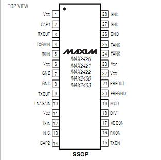
Wireless NetworksPinout Specifications
VCC to GND...................................................-0.3V to +5.5V
TXIN Input Power (330Ω system)..............................-8dBm
Voltage on TXOUT..............................-0.3V to (VCC + 1.0V)
Voltage on TXGAIN, LNAGAIN, TXON,
RXON, VCOON, DIV1, MOD..................-0.3V to (VCC + 0.3V)
RXIN Input Power......................................................10dBm
TANK, TANK Input Power............................................2dBm
Continuous Power Dissipation (TA= +70
SSOP (derate 9.50mW/°C above +70°C)..............762mW
Operating Temperature Rang
MAX242_EAI/MAX246_EAI........................-40°C to +85°C
Junction Temperature..............................................+150°C
Storage Temperature Range....................-65°C to +165°C
Lead Temperature (soldering, 10s)............................+300
DescriptionThe MAX2420/MAX2421/MAX2422/MAX2460/MAX2463 are highly integrated front-end ICs that provide the lowest cost solution for cordless phones and ISM-band radios operating in the 900MHz band. All MAX2420/MAX2421/MAX2422/MAX2460/MAX2463 devices incorporate transmit and receive image-reject mixers to reduce filter cost.
MAX2420/MAX2421/MAX2422/MAX2460/MAX2463 operate with a +2.7V to +4.8V power supply, allowing direct connection to a threecell battery stack. The receive path incorporates an adjustable-gain LNA and an image-reject downconverter with 35dB image suppression. These features yield excellent combined downconverter noise figure (4dB) and high linearity with an input third-order intercept point (IP3) of up to +2dBm.
The MAX2420/MAX2421/MAX2422/MAX2460/MAX2463 transmitter consists of a variable-gain IF amplifier with more than 35dB control range, an image-reject upconverter with 35dB image rejection, and a power amplifier (PA) predriver that produces up to +2dBm (in some applications serving as the final power stage). All devices include an on-chip local oscillator (LO), requiring only an external varactor-tuned LC tank for operation.
The integrated divide-by-64/65 dual-modulus prescaler can also be set to a direct mode, in which it acts as an LO buffer amplifier. Four separate power down inputs can be used for system power management, including a 0.5µA shutdown mode. These parts are compatible with commonly used modulation schemes such as FSK, BPSK, and QPSK, as well as frequency hopping and direct sequence spread-spectrum systems. All MAX2420/MAX2421/MAX2422/MAX2460/MAX2463 devices come in a 28-pin SSOP package.
For applications using direct VCO or BPSK transmit modulation, as well as receive image rejection, consult the MAX2424/MAX2426 data sheet. For receive only devices, refer to the MAX2440/MAX2441/MAX2442 data sheet.

 MAX2463 Data Sheet


