Features: 800MHz to 1000MHz RF Frequency Range*
39dBm Constant OIP3 (Over All Gain Settings)
23.5dBm Output 1dB Compression Point
15.5dB Typical Gain at Maximum Gain Setting
0.15dB Gain Flatness Over 100MHz Bandwidth
4.5dB Noise Figure at Maximum Gain Setting
(Using 1 Attenuator)
Two Gain-Control Ranges: 22dB and 44dB
Analog Gain Control
Single +5V Supply Voltage
Pin Compatible with MAX2057, 1700MHz to
2500MHz RF VGA
External Current-Setting Resistors Provide Option
for Operating VGA in Reduced-Power/Reduced-
Performance Mode
Lead-Free Package AvailableApplicationGSM 850/GSM 900 2G and 2.5G EDGE Base-Station Transmitters and Power Amplifiers
Cellular cdmaOne™, cdma2000, and Integrated
Digital Enhanced Network (iDEN) Base-Station
Transmitters and Power Amplifiers
W-CDMA 850MHz and Other 3G Base-Station
Transmitters and Power Amplifiers
Transmitter Gain Control
Receiver Gain Control
Broadband Systems
Automatic Test Equipment
Digital and Spread-Spectrum Communication
Systems
Microwave Terrestrial Links
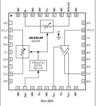
Pinout Specifications
VCC to GND.............................................................-0.3V to +5.5V
VCNTLto GND (with VCCapplied)....................................0 to 4.75V
Current into VCNTLPin (VCCgrounded).................................40mA
All Other Pins to GND....................................-0.3V to (VCC+ 0.3V)
RF Input Power (IN, IN_A, ATTN_OUT, OUT_A).................+20dBm
RF Input Power (AMP_IN).................................................+12dBm
JA(natural convection).....................................................35°C/W
JA(1m/s airflow)...............................................................31°C/W
JA(2.5m/s airflow)............................................................29°C/W
JC(junction to exposed paddle).......................................10°C/W
Operating Temperature Range.............................-40°C to +85°C
Storage Temperature Range..............................-65°C to +150°C
Junction Temperature........................................................+150°C
Lead Temperature (soldering, 10s)...................................+300°C
DescriptionThe MAX2056 general-purpose, high-performance vari- able-gain amplifier (VGA) is designed to operate in the 800MHz to 1000MHz frequency range*. This device fea-tures 15.5dB of gain, 4.5dB of noise figure, and an out- put 1dB compression point of 23.5dBm. The MAX2056 also provides an exceptionally high OIP3 level of 39dBm, which is maintained over the entire attenuation range. In addition, the on-chip analog attenuators yield infinite control and high attenuation accuracy over selectable 22dB or 44dB control ranges. Each of these features makes the MAX2056 an ideal VGA for cellular band GSM, cdma2000®, W-CDMA, and iDEN®transmit-ter and power amplifier AGC circuits.
The MAX2056 is pin compatible with the MAX2057 1700MHz to 2500MHz VGA, making this family of amplifiers ideal for applications where a common PC board layout is used for both frequency bands.
The MAX2056 operates from a single +5V supply and is available in a compact 36-pin thin QFN package (6mm x 6mm x 0.8mm) with an exposed pad. Electrical per- formance is guaranteed over the extended -40°C to +85°C temperature range.

 MAX2056 Data Sheet


