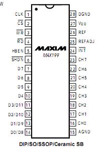
Features: © 12-Bit Resolution, 1/2LSB Linearity
© Single +5V Operation
© Software-Selectable Input Ranges:
±VREF, ±VREF/2, 0V to VREF, 0V to VREF/2
© Internal 4.096V or External Reference
© Fault-Protected Input Multiplexer (±16.5V)
© 8 Analog Input Channels
© 6s Conversion Time, 100ksps Sampling Rate
© Internal or External Acquisition Control
© Two Power-Down Modes
© Internal or External ClockApplicationIndustrial-Control Systems
Robotics
Data-Acquisition Systems
Automatic Testing Systems
Medical Instruments
TelecommunicationsPinout SpecificationsVDD to AGND...................................................................-0.3V to +7V
AGND to DGND.............................................................-0.3V to +0.3V
REF to AGND......................................................-0.3V to (VDD + 0.3V)
REFADJ to AGND................................................-0.3V to (VDD + 0.3V)
Digital Inputs to DGND......................................-0.3V to (VDD + 0.3V)
Digital Outputs to DGND....................................-0.3V to (VDD + 0.3V)
CH0CH7 to AGND ................................................................±16.5V
Continuous Power Dissipation (TA = +70°C)
Narrow Plastic DIP (derate 14.29mW/°C above +70°C)...1143mW
Wide SO (derate 12.50mW/°C above +70°C)..................1000mW
SSOP (derate 9.52mW/°C above +70°C) ..........................762mW
Narrow Ceramic SB (derate 20.00mW/°C above +70°C)..1600mW
Operating Temperature Ranges
MAX199_C_ _ ..........................................................0°C to +70°C
MAX199_E_ _........................................................-40°C to +85°C
MAX199_M_ _......................................................-55°C to +125°C
Storage Temperature Range ................................-65°C to +150°C
Lead Temperature (soldering, 10sec) ..................................+300°CDescriptionThe MAX199 multi-range, 12-bit data-acquisition system (DAS) requires only a single +5V supply for operation,and converts analog signals up to ±4V at its inputs. This system provides eight analog input channels that are independently software programmable for a variety of
ranges: ±V
REF, ±V
REF/2, 0V to V
REF, or 0V to V
REF/2.This increases effective dynamic range to 14 bits, and provides the user flexibility to interface 4mA-to-20mA,±12V, and ±15V powered sensors to a single +5V system.In addition, the converter is fault-protected to±16.5V; a fault condition on any channel will not affect the conversion result of the selected channel. Other features include a 5MHz bandwidth track/hold, 100ksps throughput rate, internal/external clock, internal/external acquisition control, 8+4 parallel interface, and operation with an internal 4.096V or external reference.
A hardware SHDN pin and two programmable powerdown modes (STBYPD, FULLPD) provide low-current shutdown between conversions. In STBYPD mode, the reference buffer remains active, eliminating start-up delays.
The MAX199 employs a standard microprocessor (P)interface. Its three-state data I/O interface is configured to operate with 8-bit data buses, and data-access and bus-release timing specifications are compatible with most popular Ps. All logic inputs and outputs are TTL/CMOS compatible.
The MAX199 is available in 28-pin DIP, wide SO, SSOP,and ceramic SB packages.
For a different combination of input ranges (±10V, ±5V,0V to 10V, 0V to 5V), see the MAX197 data sheet. For 12-bit bus interfaces, see the MAX196/MAX198 data sheet.

 MAX199 Data Sheet


