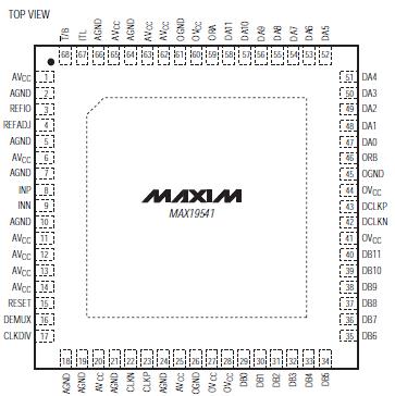
Features: `125Msps Conversion Rate
`SNR = 65dB, fIN = 100MHz at 125Msps
`SFDR = 77dBc, fIN = 100MHz at 125Msps
`±0.7 LSB INL, ±0.25 DNL (typ)
`861mW Power Dissipation at 125Msps
`On-Chip Selectable Divide-by-2 Clock Input
`Parallel or Demux Parallel Digital CMOS Outputs
`Reset Option for Synchronizing Multiple ADCs
`Data Clock Output
`Offset Binary or Two's-Complement Output
`Evaluation Kit Available (MAX19541EVKIT)Application·Base-Station Power Amplifier Linearization
·Cable Head-End Receivers
·Wireless and Wired Broadband Communication
·Communications Test Equipment
·Radar and Satellite SubsystemsPinout Specifications
AVCC to AGND .................................................-0.3V to +2.1V
OVCC to OGND ................................................-0.3V to +2.1V
AVCC to OVCC ..................................................-0.3V to +2.1V
AGND to OGND .................................................-0.3V to +0.3V
Analog Inputs (INP, INN) to AGND........-0.3V to (AVCC + 0.3V)
All Digital Inputs to AGND.....................-0.3V to (AVCC + 0.3V)
REFIO, REFADJ to AGND........................-0.3V to (AVCC + 0.3V)
All Digital Outputs to OGND .................-0.3V to (OVCC + 0.3V)
Maximum Current into Any Pin ....................................±50mA
ESD on All Pins (Human Body Model)..........................±2000V
Continuous Power Dissipation (TA = +70°C)
68-Pin QFN (derate 41.7mW/°C above +70°C) .......3333mW
Operating Temperature Range .....................-40°C to +85°C
Junction Temperature..................................................+150°C
Storage Temperature Range .......................-60°C to +150°C
Lead Temperature (soldering, 10s) .............................+300°C
Stresses beyond those listed under "Absolute Maximum Ratings" may cause permanent damage to the device. These are stress ratings only, and functional operation of the device at these or any other conditions beyond those indicated in the operational sections of the specifications is not implied. Exposure to absolute maximum rating conditions for extended periods may affect device reliability.
DescriptionThe MAX19541 monolithic 12-bit, 125Msps analog-todigital converter (ADC) is optimized for outstanding dynamic performance at high-IF frequencies of 300MHz and beyond. This device operates with conversion rates up to 125Msps while consuming only 861mW.
At 125Msps and an input frequency of 240MHz, the MAX19541 achieves a spurious-free dynamic range (SFDR) of 71.5dBc. The MAX19541 features an excellent signal-to-noise ratio (SNR) of 65.4dB at 10MHz that remains flat (within 3dB) for input tones up to 250MHz. This makes the MAX19541 ideal for wideband applications such as power-amplifier predistortion in cellular base-station transceiver systems.
The MAX19541 operates in either parallel mode where the data outputs appear on a single parallel port at the sampling rate, or in demux parallel mode, where the outputs appear on two separate parallel ports at one-half the sampling rate. See the Mode of Operation section.
The MAX19541 operates on a single 1.8V supply. The analog input is differential and can be AC- or DC-coupled. The ADC also features a selectable on-chip divide-by-2 clock circuit that allows clock frequencies as high as 250MHz. This helps to reduce the phase noise of the input clock source, allowing for higher dynamic performance. For best performance, a differential LVPECL sampling clock is recommended.
The digital outputs are CMOS compatible and the data format can be selected to be either two's complement or offset binary. A pin-compatible, 12-bit, 170Msps version of the MAX19541 is also available. Refer to the MAX19542 data sheet for more information.
The MAX19541 is available in a 68-pin QFN with exposed paddle (EP) and is specified over the extended (-40°C to +85°C) temperature range.

 MAX19541 Data Sheet


