Features: 500kHz/1MHz Current-Mode PWM Step-Up Regulator Up to +13V Main High-Power Output±1% Accurate High Efficiency (91%)
Dual Regulated Charge-Pump Outputs(MAX1778/MAX1880/MAX1881/MAX1882 only) Up to +40V Positive Charge-Pump Output Up to -40V Negative Charge-Pump Output
Low-Dropout 40mA Linear Regulator(MAX1778/MAX1881/MAX1883/MAX1884 only) Up to +15V LDO Input
Optional Higher Current with External Transistor
2.7V to 5.5V Input Supply
Internal Supply Sequencing and Soft-Start
Power-Ready Output
Adjustable Fault-Detection Latch
Thermal Protection (+160°C)
0.1A Shutdown Current
0.7mA IN Quiescent Current
Ultra-Small External Components
Thin TSSOP Package (1.1mm max height)
ApplicationTFT LCD Notebook Displays
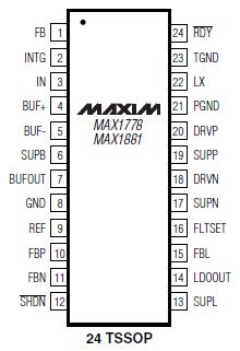
TFT LCD Desktop Monitor PanelsPinout Specifications
IN, SHDN , TGND, FLTSET to GND............................-0.3V to +6V
DRVN to GND..........................................-0.3V to (VSUPN + 0.3V)
DRVP to GND..........................................-0.3V to (VSUPP + 0.3V)
PGND to GND....................................................................±0.3V
RDY , SUPB to GND ...............................................-0.3V to +14V
LX, SUPP, SUPN to PGND ..................................... -0.3V to +14V
SUPL to GND.........................................................-0.3V to +18V
LDOOUT to GND .................................... -0.3V to (VSUPL + 0.3V)
INTG, REF, FB, FBN, FBP to GND...................-0.3V to (VIN + 0.3V)
FBL to GND ............-0.3V to the lower of (VSUPL + 0.3V) or +6V
BUFOUT, BUF+, BUF- to GND...................-0.3V to (VSUPB + 0.3V)
Continuous Power Dissipation (TA = +70°C)
20-Pin TSSOP (derate 10.9mW/°C above +70°C) .......879mW
24-Pin TSSOP (derate 12.2mW/°C above +70°C) .......975mW
Operating Temperature Range
MAX1778EUG, MAX1883EUP ...........................-40°C to +85°C
Junction Temperature....................................................+150°C
Storage Temperature Range ........................-65°C to +150°C
Lead Temperature (soldering, 10s) ..............................+300°C
DescriptionThe MAX1778/MAX1880MAX1885 multiple-output DC-DC converters provide the regulated voltages required by active matrix thin-film transistor (TFT) liquid crystal displays (LCD) in a low-profile TSSOP package. One high-power step-up converter and two low-power charge pumps convert the 2.7V to 5.5V input voltage into three independent output voltages. A built-in linear
regulator and VCOM buffer complete the power-supply requirements.
The main step-up converter accurately generates an externally set output voltage up to 13V that can supply the display's row/column drivers. The MAX1778/MAX1880MAX1885 converter's high switching frequency and current-mode PWM architecture provide fast transient response and allow the use of small low-profile inductors and ceramic capacitors. The low-power BiCMOS control circuitry and internal 14V switch (0.35 N-channel MOSFET) enable efficiencies up to 91%.
The MAX1778/MAX1880MAX1885 dual low-power charge pumps (MAX1778/ MAX1880/MAX1881/MAX1882 only) independently regulate one positive output (VPOS) and one negative output(VNEG). These low-power outputs use external diode and capacitor stages (as many stages as required) to regulate output voltages up to +40V and-40V. A unique control scheme minimizes output ripple as well as capacitor sizes for both charge pumps.
A resistor-programmable, 40mA, low-dropout linear regulator (MAX1778/MAX1881/MAX1883/MAX1884 only) provides preregulation or postregulation for any of the supplies. For higher current applications, an external transistor can be added. Additionally, the MAX1778/MAX1880MAX1885 VCOM buffer provides a high current output that is ideal for driving the capacitive backplane of TFT LCD panels. The VCOM buffer's output voltage is preset with an internal 50% resistive-divider or can be externally adjusted for other voltages.
The MAX1778/MAX1880MAX1885 are protected against output undervoltage and thermal overload conditions by a latched fault detection circuit that shuts down the device. All devices are available in the ultrathin TSSOP package (1.1mm max height).

 MAX1881 Data Sheet


