Features: One 300mA Low-Noise LDO
Four 150mA Low-Noise LDOs
45VRMS Noise from 10Hz to 100kHz
>60dB Crosstalk Isolation Below 10kH
>60dB PSRR Below 10kHz
125mV (max) Dropout (OUT1 at 200mA)
100mV (max) Dropout (OUT25 at 100mA)
Programmable Output Voltages 1.8V to 3.3V in 32 Steps
140ms (min) Reset Timer
SPI- or I2C-Compatible Serial Interface
Push-On/Push-Off Control Logic
Two 150mA General Purpose Open-Drain Outputs
Overcurrent and Thermal Protection (all LDOs)
1A Shutdown Current
20-Pin Thermally-Enhanced TSSOP or QFN Packages
ApplicationCDMA Cellular/PCS Handsets
PDAs, Palmtops, and Handy-Terminals
Single-Cell Li+ Systems
2- or 3-Cell NiMH, NiCd, or Alkaline Systems
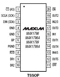
Pinout Specifications
OFF, DR1, DR2 to GND............................................-0.3V to +6V
IN1, IN2/3, IN4/5, DIN (SDA) to GND .....................-0.3V to +6V
SCLK (SCK), BP, ON to GND....................................-0.3V to +6V
RSO, ONO to GND .................................-0.3V to (VOUT1 + 0.3V)
PGND to GND....................................................................±0.3V
OUT1, CS (AS) to GND ..............................-0.3V to (VIN1 + 0.3V)
OUT2, OUT3 to GND...............................-0.3V to (VIN2/3 + 0.3V)
OUT4, OUT5 to GND...............................-0.3V to (VIN4/5 + 0.3V)
Continuous Sink Current
DR1, DR2...............................................................100mARMS
RSO................................................................................25mA
Continuous Power Dissipation (TA = +70°C)
20-Pin QFN (derate 20mW/°C above +70°C) ................1.6W
20-Pin TSSOP (derate 26mW/°C above +70°C) ............2.1W
Operating Temperature Range ........................-40°C to +85°C
Junction Temperature.....................................................+150°C
Storage Temperature Range ..........................-65°C to +150°C
Lead Temperature (soldering, 10s) ................................+300°C
DescriptionThe MAX1798/MAX1798A/MAX1799/MAX1799A system power supplies are designed specifically for CDMA cellular/ PCS handsets. Each device contains five lowdropout
linear regulators (LDOs), a 140ms (min) reset timer, a serial interface, push-on/push-off control logic, and two general-purpose open-drain outputs. Only the serial interface is different between the MAX1798/MAX1798A/MAX1799/MAX1799A: the MAX1798/MAX1798A feature an SPI™-compatible serial interface, and the MAX1799/MAX1799A feature an I2C™-compatible interface. The "A" parts have a -13% reset threshold, the non-A parts have a 9.5% threshold. The "A" parts have a 175 delay on a reset-triggered shutdown, the non-A shutdown instantly.
Each linear regulator features extremely low dropout voltage, specified at two-thirds of the maximum output current. LDO1 is rated for 300mA, while LDOs 25 are each rated for 150mA. All LDOs are optimized for low noise and isolation. Each LDO can be individually enabled and disabled through the serial port, as well as individually programmed to any of 32 voltages from 1.8V to 3.3V.
The MAX1798/MAX1798A/MAX1799/MAX1799As' wide 2.5V to 5.5V input voltage range makes them compatible with a wide range of input supplies, including a single lithium-ion (Li+) cell battery. Both devices are available in thermally-enhanced 20-pin TSSOP and QFN exposed pad (EP) packages. Evaluation kits in TSSOP (MAX1798EVKIT and MAX1799EVKIT) are available to facilitate designs.

 MAX1799 Data Sheet


