Features: ` Three Integrated DC-DC Converters
` 250kHz Current-Mode PWM Boost Regulator
Up to +13V Main High-Power Output
±1% Accuracy
High Efficiency (91%)
` Dual Charge-Pump Outputs
Up to +40V Positive Charge-Pump Output
Down to -40V Negative Charge-Pump Output
` Internal Supply Sequencing
` Internal Power MOSFETs
` +2.7V to +5.5V Input Supply
` 0.1A Shutdown Current
` 0.5mA Quiescent Current
` Internal Soft-Start
` Power-Ready Output
` Ultra-Small External Components
` Thin TSSOP Package (1.1mm max)ApplicationTFT Active-Matrix LCD Displays
Passive-Matrix LCD Displays
PDAs
Digital-Still Cameras
CamcordersPinout Specifications
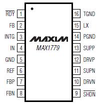
IN, SHDN, TGND to GND......................................-0.3V to +6V
DRVN to GND......................................-0.3V to (VSUPN + 0.3V)
DRVP to GND......................................-0.3V to (VSUPP + 0.3V)
PGND to GND...............................................................±0.3V
RDY to GND .....................................................-0.3V to +14V
LX, SUPP, SUPN to PGND .................................-0.3V to +14V
INTG, REF, FB, FBN, FBP to GND..............-0.3V to (VIN + 0.3V)
Continuous Power Dissipation (TA = +70°C)
16-Pin TSSOP (derate 9.4mW/°C above +70°C) .....755mW
Operating Temperature Range
MAX1779EUE ..............................................-40°C to +85°C
Junction Temperature................................................+150°C
Storage Temperature Range .....................-65°C to +150°C
Lead Temperature (soldering, 10s) ...........................+300°C
Stresses beyond those listed under "Absolute Maximum Ratings" may cause permanent damage to the device. These are stress ratings only, and functional operation of the device at these or any other conditions beyond those indicated in the operational sections of the specifications is not implied. Exposure to absolute maximum rating conditions for extended periods may affect device reliability.
DescriptionThe MAX1779 triple-output DC-DC converter provides highly efficient regulated voltages required by small active matrix, thin-film transistor (TFT) liquid-crystal displays (LCDs). One high-power DC-DC converter and two low-power charge pumps convert the +2.7V to +5.5V input supply voltage into three independent output voltages.
The primary high-power DC-DC converter generates a boosted output voltage (VMAIN) up to 13V that is regulated within ±1%. The low-power BiCMOS control circuitry and the low on-resistance (1) of the integrated power MOSFET allows efficiency up to 91%. The 250kHz current-mode pulse-width modulation (PWM) architecture provides fast transient response and allows the use of ultra-small inductors and ceramic capacitors.
The dual charge pumps independently regulate one positive output (VPOS) and one negative output (VNEG).These low-power outputs use external diode and capacitor stages (as many stages as required) to regulate output voltages up to +40V and down to -40V. A proprietary regulation algorithm minimizes output ripple,as well as capacitor sizes for both charge pumps.
The MAX1779 is available in the ultra-thin TSSOP package (1.1mm max height).

 MAX1779 Data Sheet


