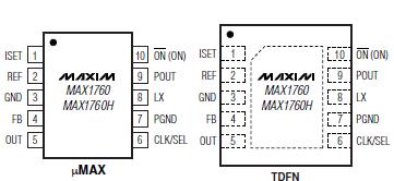
Features: `Up to 94% Efficiency
`0.7V to 5.5V Input Range
`Up to 800mA Output
`Fixed 3.3V Output (or Adjustable from 2.5V to 5.5V)
`PWM Synchronous-Rectified Topology
`Low-Noise, Constant-Frequency Operation (1MHz)
`0.1A Logic-Controlled Shutdown
`Synchronizable Switching Frequency
`Adjustable Current Limit
`Adjustable Soft-Start
`10-Pin MAX Package
`10-Pin 3mm x 3mm TDFN PackageApplication·Digital Cordless Phones
·PCS Phones
·Wireless Handsets
·Hand-Held Instruments
·Palmtop Computers
·Personal Communicators
·Two-Way PagersPinout Specifications
ON, ON, OUT, CLK/SEL to GND ...............................-0.3V to +6V
PGND to GND....................................................................±0.3V
LX to PGND ............................................-0.3V to (VPOUT + 0.3V)
POUT to OUT......................................................................±0.3V
REF, FB, ISET, POUT to GND......................-0.3V to (VOUT + 0.3V)
Continuous Power Dissipation (TA = +70°C)
10-Pin MAX (derate 5.6mW/°C above +70°C) .............444mW
10-Pin TDFN (derate 24.4mV°C above +70°C) ............1951mW
Operating Temperature Range .........................-40°C to +85°C
Junction Temperature......................................................+150°C
Storage Temperature Range ...........................-65°C to +150°C
Lead Temperature (soldering, 10s) .................................+300°C
Stresses beyond those listed under "Absolute Maximum Ratings" may cause permanent damage to the device. These are stress ratings only, and functional operation of the device at these or any other conditions beyond those indicated in the operational sections of the specifications is not implied. Exposure to absolute maximum rating conditions for extended periods may affect device reliability.
DescriptionThe MAX1760/MAX1760H are high-efficiency, low-noise, step-up DC-DC converters intended for use in batterypowered wireless applications. They combine low quiescent supply current (100A) with a high 1MHz operating frequency. Small external components and tiny 10-pin TDFN and MAX packages make this device an excellent choice for small hand-held applications. The MAX1760 is activated by a logic-low ON signal while the MAX1760H is activated by a logic-high ON input.
Both devices use a synchronous-rectified pulse-widthmodulation (PWM) boost topology to generate 2.5V to 5.5V outputs from a wide range of inputs, such as 1 to 3 alkaline or NiCd/NiMH cells or a single lithium-ion (Li+) cell. Proprietary Idle-Mode™ circuitry significantly improves light-load efficiency and smoothly transitions to fixed-frequency PWM operation at higher load currents.
Low-noise, forced-PWM mode is available for applications requiring constant-frequency operation at all load currents. PWM operation can also be synchronized to an external clock to protect sensitive frequency bands in communications equipment. Analog soft-start and adjustable current limit permit optimization of efficiency, external component size, and output voltage ripple.

 MAX1760H Data Sheet


