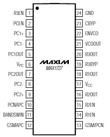
Features: `+3.1V to +5.5V Input Range
`One 2.90V, 100mA Low IQ LDO
`One 2.75V, 50mA Low IQ LDO
`One 2.75V, 20mA Low IQ LDO
`Low-Noise LDOs <90VRMS from 10Hz to 100kHz >80dB Crosstalk Isolation at 10kHz >70dB PSRR at 1kHz
`±5% Accuracy Over Line, Load, and Temperature
`Three 2.5 Switched Outputs
`Current and Thermal Limit
`Two Undedicated Op Amps Rail-to-Rail CMR Inputs and Outputs >120dB Channel Separation >85dB PSRR at 1kHz
`10A (max) Shutdown CurrentApplication·GSM Cellular or PCN Handsets
·Single-Cell Li+ Systems
·3-Cell NiMH, NiCD, or Alkaline SystemsPinout Specifications
VCC, VPC to GND......................................................-0.3V to +7V
PC1-, PC1+, PC2-, PC2+ to GND ............................-0.3V to +7V
GSM/PCN, BANDSWIN to GND ..............................-0.3V to +7V
PC1OUT, PC2OUT to GND ....................................-0.3V to +7V
R1OUT, R2OUT, R3BYP to GND..................-0.3V to (VCC + 0.3V)
R3OUT, CBYP to GND ..........................-0.3V to (VR3BYP + 0.3V)
R1EN, R2EN, R3EN, ENVCO,
PCEN to GND.............................................-0.3V to (VCC + 0.3V)
VCOOUT to GND..................................-0.3V to (VR3OUT + 0.3V)
GSMAPC, PCNAPC to GND..............-0.3V to (VBANDSWIN + 0.3V)
Continuous Power Dissipation (TA = +70)
24-Pin TSSOP (derate 12.2mW/ above +70) ...........975mW
Operating Temperature Range ...........................-40 to +85
Junction Temperature......................................................+150
Storage Temperature Range .............................-65 to +150
Lead Temperature(soldering, 10s) ..................................+300
Stresses beyond those listed under "Absolute Maximum Ratings" may cause permanent damage to the device. These are stress ratings only, and functional operation of the device at these or any other conditions beyond those indicated in the operational sections of the specifications is not implied. Exposure to absolute maximum rating conditions for extended periods may affect device reliability.
DescriptionThe MAX1727 is a radio frequency (RF) power-management IC intended for Global Satellite Mobile (GSM) communication cellular and personal cellular network (PCN) handsets using a single lithium-ion (Li+) cell battery with inputs from +3.1V to +5.5V. The IC contains four low-noise, low-dropout (LDO) linear regulators to provide all the supply voltage requirements for the RF portion of the handset, and two high-speed, wide-bandwidth op amps for the power amplifier (PA) power control loop.
Each LDO has its own individual on/off control to maximize design flexibility. All LDOs are internally trimmed to a fixed output voltage and are optimized for low noise and high crosstalk isolation. LDO1 (R1OUT) is rated for 100A and is optimized for lowest quiescent current. It is intended to power the transmitter, receiver, and synthesizer. LDO2 (R2OUT) is rated for 50mA. It is intended to power the TCXO, GSM, and PCN highpower voltage-controlled oscillators (VCOs). LDO3 (R3OUT) is rated for 20mA and is optimized to suppress line transients. It is intended to power the UHF offset VCO. LDO3 has an auxiliary 2.5 switched output to allow the VCO to be powered up with precise timing. LDO4 (R3BYP) is rated for 20mA. It is intended to power this IC's reference and LDO3 for superior line rejection. LDO4 and the reference will be powered on if any of the R1EN, R2EN, and R3EN enable inputs are logic high.
The op amps have wide bandwidth, high DC accuracy, high slew rate, and Rail-to-Rail® inputs and outputs.
The op amps can sink and source 3mA, and include two 2.5 switched outputs. The op amps and switched outputs may be used independently or may be configured to provide optimized power for a PA control loop.

 MAX1727 Data Sheet


