Features: On-Chip 5A Power MOSFET
5V, 2A Output from a 3.3V Input
Fixed 3.3V or 5V Output Voltage or
Adjustable (2.5V to 5.5V)
Input Voltage Range Down to 0.7V
Low Power Consumption
1mW Quiescent Power
1A Current in Shutdown Mode
Low-Noise, Constant Frequency Operation(600kHz)
Synchronizable Switching Frequency(350kHz to 1000kHz)
Small QSOP Package
Application Routers, Servers, Workstations, Card Racks
Local 2.5V to 3.3V or 5V Conversion
Local 3.3V to 5V Conversion
3.6V or 5V RF PAs in Communications Handsets
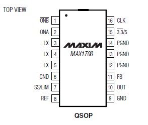
Pinout Specifications
ONA, ONB, OUT, SS/LIM, 3.3/5 to GND ..................-0.3V to +6.0V
LX to PGND ...........................................................-0.3V to +6.0V
FB, CLK, REF to GND.................................-0.3V to (VOUT + 0.3V)
PGND to GND ........................................................-0.3V to +0.3V
Continuous Power Dissipation (TA = +70°C)
16-Pin QSOP (derate 8.30mW/°C above +70°C).............667mW
Operating Temperature Range ..........................-40°C to +85°C
Junction Temperature.....................................................+150°C
Storage Temperature Range ...........................-65°C to +150°C
Lead Temperature (soldering, 10s) ................................+300°C
Stresses beyond those listed under "Absolute Maximum Ratings" may cause permanent damage to the device. These are stress ratings only, and functional operation of the device at these or any other conditions beyond those indicated in the operational sections of the specifications is not implied. Exposure to absolute maximum rating conditions for extended periods may affect device reliability.
DescriptionThe MAX1708 sets a new standard of space savings for high-power, step-up DC-DC conversion. It delivers up to 10W at a fixed (3.3V or 5V) or adjustable (2.5V to 5.5V) output, using an on-chip power MOSFET from a+0.7V to +5V supply.
Fixed-frequency PWM operation ensures that the switching noise spectrum is constrained to the 600kHz fundamental and its harmonics, allowing easy postfiltering for noise reduction. External clock synchronization capability allows for even tighter noise spectrum control.Quiescent power consumption is less than 1mW to extend operating time in battery-powered systems.
Two control inputs (ONA, ONB) allow simple push-on,push-off control through a single momentary push-button switch, as well as conventional on/off logic control.The MAX1708 also features programmable soft-start and current limit for design flexibility and optimum performance with batteries. The maximum RMS switch current rating is 5A. For a device with a higher (10A) switch current rating, refer to the MAX1709 data sheet.

 MAX1708 Data Sheet


