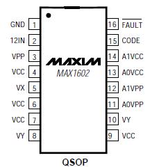
Features: ` Supports a Single PC Card/CardBus Socket
` 1A, 0.25 Max 3.3V VCC Switch
1A, 0.25 Max 5V VCC Switch
` Soft Switching for Low Inrush Surge Current
` Overcurrent Protection
` Overcurrent/Thermal-Fault Flag Output
` Thermal Shutdown at Tj = +150°C
` Independent Internal Charge Pumps
` Break-Before-Make Switching Action
` 11A Max Standby Supply Current
` 5V and 12V Not Required for Low-RDS(ON) 3.3V Switching
` Complies with PCMCIA 3V/5V Switching Specifications
` Super-Small 16-Pin QSOP Package
` Code Compatible with:
Cirrus CL-PD67XX Family
Databook DB86184
Intel 82365SL (industry-standard coding)ApplicationData Loggers
Handy-Terminals
Docking Stations
PCMCIA Read/Write DrivesPinout Specifications
Inputs/Outputs to GND
(VX, VY, VCC) (Note 1) .........................................-0.3V, +6V
VPP Input/Output to GND
(12IN, VPP) (Note 1) ..........................................-0.3V, +15V
Logic Inputs to GND (A0VCC, A1VCC,
A0VPP, A1VPP) (Note 1)........................................-0.3V, +6V
CODE Input to GND ...................................-0.3V, (VY + 0.3V)
VCC Output Current (Note 2).............................................4A
VPP Output Current (Note 2).......................................260mA
VCC Short Circuit to GND .....................................Continuous
VPP Short Circuit to GND ......................................Continuous
Continuous Power Dissipation (TA = +70°C)
QSOP (derate 8.3mW/°C above +70°C) ..................667mW
Operating Temperature Range
MAX1602EEE................................................-40°C to +85°C
Storage Temperature Range .....................-65°C to +160°C
Lead Temperature (soldering, 10sec) ........................+300°C
Note 1: There are no parasitic diodes between any of these pins, so there are no power-up sequencing restrictions (for example,logic input signals can be applied even if all of the supply voltage inputs are grounded).
Note 2: VCC and VPP outputs are internally current limited. See the Electrical Characteristics.
Stresses beyond those listed under "Absolute Maximum Ratings" may cause permanent damage to the device. These are stress ratings only, and functional operation of the device at these or any other conditions beyond those indicated in the operational sections of the specifications is not implied. Exposure to absolute maximum rating conditions for extended periods may affect device reliability.
DescriptionThe MAX1602 DC power-switching IC contains a network of low-resistance MOSFET switches that deliver selectable VCC and VPP voltages to a single CardBus or PC Card host socket. Key features include lowresistance switches, small packaging, soft-switching action, and compliance with PCMCIA specifications for 3V/5V switching. 3.3V-only power switching for fast,32-bit CardBus applications is supported in two ways:low-resistance 3.3V switches allow high 3.3V load currents (up to 1A); and completely independent internal charge pumps let the 3.3V switch operate normally,even if the +5V and +12V supplies are disconnected or turned of to conserve power. The internal charge pumps are regulating types that draw reduced input current when the VCC switches are static. Power consumption is automatically reduced to 11A max when the outputs are high-Z or GND.
Other key features include guaranteed specifications for output current limit level, and guaranteed specifications for output rise/fall times (in compliance with PCMCIA specifications). Reliability is enhanced by thermal-overload protection, accurate current limiting, an overcurrent-fault flag output, and undervoltage lockouts.The CMOS/TTL-logic interface is flexible, and can tolerate logic input levels in excess of the positive supply rail.
The MAX1602 fits a complete CardBus/PCMCIA switch into a space-saving, 16-pin QSOP package.

 MAX1602 Data Sheet


