`PDA,
`
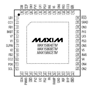
Pinout

Specifications
IN, IN45, IN6, MR, LBO, DBO, RSO, POK, SCL, SDA,
BKBT, V7, SLP, SRAD, PWM3 to GND..........................-0.3V to +6V
REF, CC_, ON_, FB_, DBI, LBI, V1, V2, RAMP, BYP,
MR to GND ...................................................-0.3V to (VIN + 0.3V)
PV1, PV2, PV3, SLPIN to IN....................................-0.3V to +0.3V
V4, V5 to GND ..........................................-0.3V to (VIN45 + 0.3V)
V6 to GND ..................................................-0.3V to (VIN6 + 0.3V)
PV1 to PG1 ............................................................-0.3V to +6.0V
PV2 to PG2 ............................................................-0.3V to +6.0V
PV3 to PG3 ............................................................-0.3V to +6.0V
LX1 Continuous Current.....................................-1.30A to +1.30A
LX2 Continuous Current.........................................-0.9A to +0.9A
LX3 Continuous Current.........................................-0.9A to +0.9A
PG1, PG2, PG3 to GND............................................-0.3V to +0.3V
V1, V2, V4, V5, V6 Output Short-Circuit Duration.........Continuous
Continuous Power Dissipation (TA = +70°C)
6mm x 6mm 40-Pin Thin QFN
(derate 26.3mW/°C above +70°C)..............................2105mW
7mm x 7mm 48-Pin Thin QFN
(derate 26.3mW/°C above +70°C)..............................2105mW
Operating Temperature Range .........................-40°C to +85°C
Junction Temperature......................................................+150°C
Storage Temperature Range ...........................-65°C to +150°C
Lead Temperature (soldering, 10s) .................................+300°C
Description
The MAX1586/MAX1587 power-management ICs are optimized for devices using Intel XScale® microprocessors, including third-generation smart cell phones, PDAs, internet appliances, and other portable devices requiring substantial computing and multimedia capability at low power.
The MAX1586/MAX1587 ICs integrate seven high-performance, low-operating-current power supplies along with supervisory and management functions. Regulator outputs include three step-down DC-DC outputs, three linear regulators, and a seventh always-on output. DC-DC converter outputs power I/O, DRAM, and the CPU core. The I/O supply can be preset to 3.3V or 3.0V, or can be adjusted to other values. The DRAM supply on the MAX1586A and MAX1587A is preset for 1.8V or 2.5V, while the MAX1586B DRAM supply is preset for 3.3V or 2.5V. The DRAM supply on all parts can also be adjusted with external resistors. The CPU core supply is serial programmed for dynamic voltage management. Linear-regulated outputs are provided for SRAM, PLL, and USIM supplies.
To minimize sleep-state quiescent current of MAX1586/MAX1587, critical power supplies have bypass "sleep" LDOs that can be activated to minimize battery drain when output current is very low. Other functions include separate on/off control for all DC-DC converters, low-battery and dead-battery detection, a reset and power-OK output, a backup-battery input, and a two-wire serial interface.
All DC-DC outputs use fast, 1MHz PWM switching and small external components. They operate with fixed-frequency PWM control and automatically switch from PWM to skip-mode operation at light loads to reduce operating current and extend battery life. The core output is capable of operating in forced-PWM mode at all loads to minimize ripple and noise. A 2.6V to 5.5V input voltage range allows 1-cell lithium-ion (Li+), 3-cell NiMH, or a regulated 5V input. The MAX1587 is available in a tiny 6mm x 6mm, 40-pin thin QFN package. The MAX1586 features an additional linear regulator (V6) for VCC_USIM and low-battery and dead-battery comparators. The MAX1586 is available in a 7mm x 7mm, 48-pin thin QFN package.

 MAX1587C Data Sheet


