MAX1449

Features: Single +3.3V Operation Excellent Dynamic Performance 58.5dB SNR at fIN = 20MHz 72dBc SFDR at fIN = 20MHz Low Power62mA (Normal Operation)5µA (Shutdown Mode) Fully Differential Analog InputWide 2Vp-p Differential Input Voltage Range400MHz -3dB Input BandwidthOn-Chip +2.048V Precisio...

product image

MAX1449 Picture
SeekIC No. : 004408917 Detail

MAX1449: Features: Single +3.3V Operation Excellent Dynamic Performance 58.5dB SNR at fIN = 20MHz 72dBc SFDR at fIN = 20MHz Low Power62mA (Normal Operation)5µA (Shutdown Mode) Fully Differential Analog...

floor Price/Ceiling Price

Part Number:
MAX1449
Supply Ability:
5000

Price Break

  • Qty
  • 1~5000
  • Unit Price
  • Negotiable
  • Processing time
  • 15 Days
Total Cost: $ 0.00

SeekIC Buyer Protection PLUS - newly updated for 2013!

  • Escrow Protection.
  • Guaranteed refunds.
  • Secure payments.
  • Learn more >>

Month Sales

268 Transactions

Rating

evaluate  (4.8 stars)

Upload time: 2024/11/27

Payment Methods

All payment methods are secure and covered by SeekIC Buyer Protection PLUS.

Notice: When you place an order, your payment is made to SeekIC and not to your seller. SeekIC only pays the seller after confirming you have received your order. We will also never share your payment details with your seller.
Product Details

Description


Features:

 Single +3.3V Operation
Excellent Dynamic Performance
        58.5dB SNR at fIN = 20MHz
        72dBc SFDR at fIN = 20MHz
Low Power
        62mA (Normal Operation)
        5µA (Shutdown Mode)
Fully Differential Analog Input
 Wide 2Vp-p Differential Input Voltage Range
 400MHz -3dB Input Bandwidth
 On-Chip +2.048V Precision Bandgap Reference
 CMOS-Compatible Three-State Outputs
 32-Pin TQFP Package
Evaluation Kit Available


Application

Ultrasound Imaging
CCD Imaging
Baseband and IF Digitization
Digital Set-Top Boxes
Video Digitizing Applications


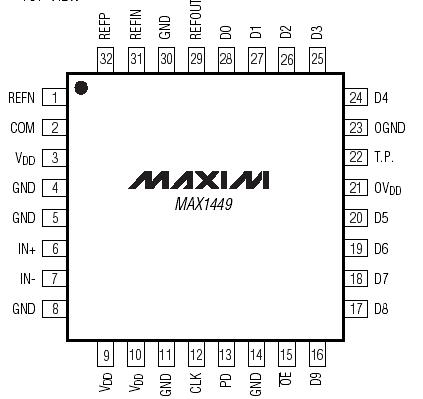
Pinout

  Connection Diagram


Specifications

VDD, OVDD to GND ...............................................-0.3V to +3.6V
OGND to GND.......................................................-0.3V to +0.3V
IN+, IN- to GND........................................................-0.3V to VDD
REFIN, REFOUT, REFP,
REFN, and COM to GND.............................-0.3V to (VDD + 0.3V)
OE, PD, CLK to GND...................................-0.3V to (VDD + 0.3V)
D9D0 to GND.........................................-0.3V to (OVDD + 0.3V)
Continuous Power Dissipation (TA = +70°C)
32-Pin TQFP (derate 11.1mW/°C above +70°C).............889mW
Operating Temperature Range .........................-40°C to +85°C
Junction Temperature.....................................................+150°C
Storage Temperature Range ...........................-60°C to +150°C
Lead Temperature (soldering, 10s) ................................+300°C


Description

The MAX1449 +3.3V, 10-bit analog-to-digital converter (ADC) features a fully differential input, a pipelined 10- stage ADC architecture with wideband track-and-hold (T/H), and digital error correction incorporating a fully differential signal path. The ADC is optimized for lowpower, high-dynamic performance in imaging and digital communications applications. The converter operates from a single +2.7V to +3.6V supply, consuming only 186mW while delivering a 58.5dB (typ) signalto- noise ratio (SNR) at a 20MHz input frequency. The fully differential input stage has a -3dB 400MHz bandwidth and may be operated with single-ended inputs. In addition to low operating power, the MAX1449 features a 5µA power-down mode for idle periods.

An internal +2.048V precision bandgap reference is used to set the ADC's full-scale range. A flexible reference structure allow's the user to supply a buffered, direct, or externally derived reference for applications requiring increased accuracy or a different input voltage range.

Lower speed, pin-compatible versions of the MAX1449 are also available. Refer to the MAX1444 data sheet for a 40Msps version, the MAX1446 data sheet for a 60Msps version, and the MAX1448 data sheet for 80Msps.

The MAX1449 has parallel, offset binary, CMOS-compatible, three-state outputs that can be operated from +1.7V to +3.6V to allow flexible interfacing. The device is available in a 5mm x 5mm 32-pin TQFP package and is specified over the extended industrial (-40°C to +85°C) temperature range.


Customers Who Bought This Item Also Bought

Margin,quality,low-cost products with low minimum orders. Secure your online payments with SeekIC Buyer Protection.
Isolators
RF and RFID
Crystals and Oscillators
Audio Products
Programmers, Development Systems
Batteries, Chargers, Holders
View more