MAX1434ECQ

Features: · Excellent Dynamic Performance 61dB SNR at 5.3MHz 84dBc SFDR at 5.3MHz 94dB Channel Isolation· Ultra-Low Power 96mW per Channel (Normal Operation)· Serial LVDS Outputs· Pin-Selectable LVDS/SLVS (Scalable Low-Voltage Signal) Mode· LVDS Outputs Support Up to 30 Inches FR-4 Backplane Conne...

product image

MAX1434ECQ Picture
SeekIC No. : 004408897 Detail

MAX1434ECQ: Features: · Excellent Dynamic Performance 61dB SNR at 5.3MHz 84dBc SFDR at 5.3MHz 94dB Channel Isolation· Ultra-Low Power 96mW per Channel (Normal Operation)· Serial LVDS Outputs· Pin-Selectable LVD...

floor Price/Ceiling Price

Part Number:
MAX1434ECQ
Supply Ability:
5000

Price Break

  • Qty
  • 1~5000
  • Unit Price
  • Negotiable
  • Processing time
  • 15 Days
Total Cost: $ 0.00

SeekIC Buyer Protection PLUS - newly updated for 2013!

  • Escrow Protection.
  • Guaranteed refunds.
  • Secure payments.
  • Learn more >>

Month Sales

268 Transactions

Rating

evaluate  (4.8 stars)

Upload time: 2024/11/27

Payment Methods

All payment methods are secure and covered by SeekIC Buyer Protection PLUS.

Notice: When you place an order, your payment is made to SeekIC and not to your seller. SeekIC only pays the seller after confirming you have received your order. We will also never share your payment details with your seller.
Product Details

Description


Features:

· Excellent Dynamic Performance
    61dB SNR at 5.3MHz
    84dBc SFDR at 5.3MHz
    94dB Channel Isolation
· Ultra-Low Power 96mW per Channel (Normal Operation)
· Serial LVDS Outputs
· Pin-Selectable LVDS/SLVS (Scalable Low-Voltage Signal) Mode
· LVDS Outputs Support Up to 30 Inches FR-4 Backplane Connections
· Test Mode for Digital Signal Integrity
· Fully Differential Analog Inputs
· Wide Differential Input Voltage Range (1.4VP-P)
· On-Chip 1.24V Precision Bandgap Reference
· Clock Duty-Cycle Equalizer
· Compact, 100-Pin TQFP Package with Exposed Paddle
· Evaluation Kit Available (Order MAX1434EVKIT)


Application

·Ultrasound and Medical Imaging
·Instrumentation
·Multichannel Communications


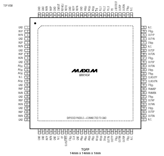
Pinout

  Connection Diagram


Specifications

AVDD to GND..........................................................-0.3V to +2.0V
CVDD to GND .........................................................-0.3V to +3.6V
OVDD to GND .........................................................-0.3V to +2.0V
IN_P, IN_N to GND....................................-0.3V to (AVDD + 0.3V)
CLK to GND...............................................-0.3V to (CVDD + 0.3V)
OUT_P, OUT_N, FRAME_,
CLKOUT_ to GND......................................-0.3V to (OVDD + 0.3V)
DT, SLVS/LVDS, LVDSTEST, PLL_, T/B,
REFIO, REFADJ, CMOUT to GND ................-0.3V to (AVDD + 0.3V)
Continuous Power Dissipation (TA = +70°C)
100-Pin TQFP 14mm x 14mm x 1mm
(derated 47.6mW/°C above +70°C)........................3809.5mW
Operating Temperature Range ........................-40°C to +85°C
Maximum Junction Temperature .....................................+150°C
Storage Temperature Range ..........................-65°C to +150°C
Lead Temperature (soldering, 10s) ................................+300°C


Description

The MAX1434ECQ octal, 10-bit analog-to-digital converter (ADC) features fully differential inputs, a pipelined architecture, and digital error correction incorporating a fully differential signal path. This ADC is optimized for low-power and high-dynamic performance in medical imaging instrumentation and digital communications applications. The MAX1434 operates from a 1.8V single supply and consumes only 767mW (96mW per channel) while delivering a 61dB (typ) signal-to-noise ratio (SNR) at a 5.3MHz input frequency. In addition to low operating power, the MAX1434 features a power-down mode for idle periods.

An internal 1.24V precision bandgap reference sets the full-scale range of the ADC. A flexible reference structure allows the use of an external reference for applications requiring increased accuracy or a different input voltage range. The reference architecture is optimized for low noise.

A single-ended clock controls the data-conversion process. An internal duty-cycle equalizer compensates for wide variations in clock duty cycle. An on-chip PLL generates the high-speed serial low-voltage differential signal (LVDS) clock.

The MAX1434ECQ has self-aligned serial LVDS outputs for data, clock, and frame-alignment signals. The output data is presented in two's complement or binary format. The MAX1434 offers a maximum sample rate of 50Msps. See the Pin-Compatible Versions table below for 12-bit versions. This device is available in a small, 14mm x 14mm x 1mm, 100-pin TQFP package with exposed paddle and is specified for the extended industrial (-40°C to +85°C) temperature range.


Customers Who Bought This Item Also Bought

Margin,quality,low-cost products with low minimum orders. Secure your online payments with SeekIC Buyer Protection.
RF and RFID
Boxes, Enclosures, Racks
Test Equipment
Soldering, Desoldering, Rework Products
Hardware, Fasteners, Accessories
Programmers, Development Systems
View more