Features: +3.3V Single Power Supply
67dB SNR at fIN = 5MHz
66dB SNR at fIN = 15MHz
Internal +2.048V Precision Bandgap Reference
Differential, Wideband Input T/H Amplifier
Power-Down Modes:
218mW (Reference Shutdown Mode)
10µW (Shutdown Mode)
Space-Saving 48-Pin TQFP PackageApplication Medical Ultrasound Imaging
CCD Pixel Processing
IR Focal Plane Arrays
Radar
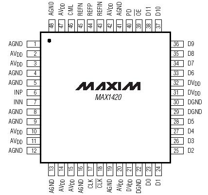
IF & Baseband DigitizationPinout Specifications
AVDD, DVDD to AGND..............................................-0.3V to +4V
DVDD, AVDD to DGND..............................................-0.3V to +4V
DGND to AGND.....................................................-0.3V to +0.3V
INP, INN, REFP, REFN, REFIN,
CML, CLK, CLK ..........................(AGND - 0.3V) to (AVDD + 0.3V)
D0D11, OE, PD .......................(DGND - 0.3V) to (DVDD + 0.3V)
Continuous Power Dissipation (TA = +70°C)
48-Pin TQFP (derate 12.5mW/°C above +70°C)..........1000mW
Operating Temperature Ranges
MAX1420CCM ......................................................0°C to +70°C
MAX1420ECM ...................................................-40°C to +85°C
Maximum Junction Temperature ...................................+150°C
Storage Temperature Range .........................-65°C to +150°C
Lead Temperature (soldering, 10s) ..............................+300°C
DescriptionThe MAX1420, +3.3V, 12-bit analog-to-digital converter (ADC) features a fully-differential input, pipelined, 12- stage ADC architecture with wideband track-and-hold (T/H) and digital error correction, incorporating a fullydifferential signal path. The MAX1420 is optimized for low-power, high dynamic performance applications in imaging and digital communications. The converter operates from a single +3.3V supply, and consumes only 221mW. The fully-differential input stage has a small signal -3dB bandwidth of 400MHz and may be operated with single-ended inputs.
An internal +2.048V precision bandgap reference sets the full-scale range of the ADC. A flexible reference structure accommodates an internal reference, or externally applied buffered or unbuffered reference for applications that require increased accuracy and a different input voltage range.
In addition to low operating power, the MAX1420 features two power-down modes: reference power-down and shutdown mode. In reference power-down, the internal bandgap reference is deactivated, which results in a typical 2mA supply current reduction. A full shutdown mode is available to maximize power savings during idle periods.
The MAX1420 provides parallel, offset binary, CMOScompatible three-state outputs.
The MAX1420 is available in a 7mm ✕ 7mm, 48-pin TQFP package, and is specified over the commercial (0°C to +70°C) and the extended industrial (-40°C to +85°C) temperature range.
Pin-compatible lower speed versions of the MAX1420 are also available. Please refer to the MAX1421 data sheet for 40Msps and the MAX1422 data sheet for 20Msps.

 MAX1420 Data Sheet


