MAX1311

Features: ` ±1 LSB INL, ±0.9 LSB DNL (max)` 84dBc SFDR, -86dBc THD, 71dB SINAD,fIN = 500kHz at -0.4dBFS` Extended Input Ranges 0 to +5V (MAX1307) -5V to +5V (MAX1311) -10V to +10V (MAX1315)` Fault-Tolerant Inputs ±6V (MAX1307) ±16.5V (MAX1311/MAX1315)` Fast 0.72s Conversion Time` 12-Bit, 20MHz Par...

product image

MAX1311 Picture
SeekIC No. : 004408770 Detail

MAX1311: Features: ` ±1 LSB INL, ±0.9 LSB DNL (max)` 84dBc SFDR, -86dBc THD, 71dB SINAD,fIN = 500kHz at -0.4dBFS` Extended Input Ranges 0 to +5V (MAX1307) -5V to +5V (MAX1311) -10V to +10V (MAX1315)` Fault-T...

floor Price/Ceiling Price

Part Number:
MAX1311
Supply Ability:
5000

Price Break

  • Qty
  • 1~5000
  • Unit Price
  • Negotiable
  • Processing time
  • 15 Days
Total Cost: $ 0.00

SeekIC Buyer Protection PLUS - newly updated for 2013!

  • Escrow Protection.
  • Guaranteed refunds.
  • Secure payments.
  • Learn more >>

Month Sales

268 Transactions

Rating

evaluate  (4.8 stars)

Upload time: 2024/11/27

Payment Methods

All payment methods are secure and covered by SeekIC Buyer Protection PLUS.

Notice: When you place an order, your payment is made to SeekIC and not to your seller. SeekIC only pays the seller after confirming you have received your order. We will also never share your payment details with your seller.
Product Details

Description


Features:

` ±1 LSB INL, ±0.9 LSB DNL (max)
` 84dBc SFDR, -86dBc THD, 71dB SINAD,fIN = 500kHz at -0.4dBFS
` Extended Input Ranges 0 to +5V (MAX1307)  -5V to +5V (MAX1311) -10V to +10V (MAX1315)
` Fault-Tolerant Inputs ±6V (MAX1307) ±16.5V (MAX1311/MAX1315)
` Fast 0.72s Conversion Time
` 12-Bit, 20MHz Parallel Interface
` Internal or External Clock
` +2.5V Internal Reference or +2.0V to +3.0V External Reference
` +5V Analog Supply, +3V to +5V Digital Supply 36mA Analog Supply Current 1.3mA Digital Supply Current Shutdown Mode
` 48-Pin TQFP Package (7mm x 7mm Footprint


Application

·Industrial Process Control and Automation
·Vibration and Waveform Analysis
·Data-Acquisition Systems


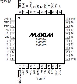
Pinout

  Connection Diagram


Specifications

AVDD to AGND ........................................................-0.3V to +6V
DVDD to DGND........................................................-0.3V to +6V
AGND to DGND.....................................................-0.3V to +0.3V
CH0, I.C. to AGND (MAX1307) .............................................±6V
CH0, I.C. to AGND (MAX1311)  .......................................±16.5V
CH0, I.C. to AGND (MAX1315) .......................................±16.5V
D0D11 to DGND ..................................-0.3V to (DVDD + 0.3V)
EOC, EOLC, RD, WRCS to DGND............-0.3V to (DVDD + 0.3V)
CONVST, CLK, SHDN, CHSHDN to DGND..-0.3V to (DVDD + 0.3V)
INTCLK/EXTCLK to AGND.........................-0.3V to (AVDD + 0.3V)
REFMS, REF, MSV to AGND.......................-0.3V to (AVDD + 0.3V)
REF+, COM, REF- to AGND.......................-0.3V to (AVDD + 0.3V)
Maximum Current into Any Pin Except AVDD,
DVDD, AGND, DGND.........................................................±50mA
Continuous Power Dissipation (TA = +70)
TQFP (derate 22.7mW/ above +70).....................1818.2mW
Operating Temperature Range ............................-40 to +85
Junction Temperature.......................................................+150
Storage Temperature Range .............................-65 to +150
Lead Temperature (soldering, 10s) .................................+300
Stresses beyond those listed under "Absolute Maximum Ratings" may cause permanent damage to the device. These are stress ratings only, and functional operation of the device at these or any other conditions beyond those indicated in the operational sections of the specifications is not implied. Exposure to absolute maximum rating conditions for extended periods may affect device reliability


Description

The MAX1307/MAX1311/MAX1315 12-bit, analog-to-digital converters (ADCs) feature a 1075ksps sampling rate, a 20MHz input bandwidth, and three analog input ranges.The MAX1307 provides a 0 to +5V input range, with ±6V fault-tolerant inputs. The MAX1311 provides a ±5V input range with ±16.5V fault-tolerant inputs. The MAX1315 provides a ±10V input range with ±16.5V fault-tolerant inputs.

The MAX1307/MAX1311/MAX1315 include an on-chip 2.5V reference. These devices also accept an external +2V to +3V reference.

All devices operate from a +4.75 to +5.25V analog supply,and a +2.7V to +5.25V digital supply. The devices consume 36mA total supply current when fully operational.A 0.62A shutdown mode is available to save
power during idle periods.

A 20MHz, 12-bit, parallel data bus provides the conversion results. An internal 15MHz oscillator, or an externally applied clock, drives conversions.

Each device is available in a 48-pin 7mm x 7mm TQFP package and operates over the extended (-40 to +85) temperature range.


Customers Who Bought This Item Also Bought

Margin,quality,low-cost products with low minimum orders. Secure your online payments with SeekIC Buyer Protection.
Crystals and Oscillators
Semiconductor Modules
Static Control, ESD, Clean Room Products
Programmers, Development Systems
View more