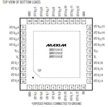
Features: ` Wide Supply Voltage RangeVCC Range of 1.65V to 5.5VVL Range of 1.2V to VCC` ESD Protection on I/O VCC Lines±15kV Human Body Model` Up to 20Mbps Throughput` Low 0.03A Typical Quiescent Current` UCSP and TQFN PackagesApplication·CMOS Logic-Level Translation·Portable Equipment·Cell Phones...
MAX13108E: Features: ` Wide Supply Voltage RangeVCC Range of 1.65V to 5.5VVL Range of 1.2V to VCC` ESD Protection on I/O VCC Lines±15kV Human Body Model` Up to 20Mbps Throughput` Low 0.03A Typical Quiescent Cu...
SeekIC Buyer Protection PLUS - newly updated for 2013!
268 Transactions
All payment methods are secure and covered by SeekIC Buyer Protection PLUS.
VCC..........................................................................-0.3V to +6V
VL.............................................................................-0.3V to +6V
I/O VCC_......................................................-0.3V to (VCC + 0.3V)
I/O VL_...........................................................-0.3V to (VL + 0.3V)
EN, MULT .................................................................-0.3V to +6V
Short-Circuit Duration I/O VL_, I/O VCC_ to GND .......Continuous
Continuous Power Dissipation (TA = +70°C)
36-Bump UCSP (derate 17.0mW/°C above +70°C) ..1361mW
40-Pin TQFN (derate 35.7mW/°C above +70°C) .......2857mW
Operating Temperature Range .......................-40°C to +85°C
Maximum Junction Temperature ...................................+150°C
Storage Temperature Range ........................-65°C to +150°C
Lead Temperature (soldering, 10s) ..............................+300°C
Stresses beyond those listed under "Absolute Maximum Ratings" may cause permanent damage to the device. These are stress ratings only, and functional operation of the device at these or any other conditions beyond those indicated in the operational sections of the specifications is not implied. Exposure to absolute maximum rating conditions for extended periods may affect device reliability.
The MAX13101E/MAX13102E/MAX13103E/MAX13108E 16-bit bidirectional CMOS logic-level translators provide the level shifting necessary to allow data transfer in multivoltage systems. These devices are inherently bidirectional due to their design and do not require the use of a direction input. Externally applied voltages, VCC and VL, set the logic levels on either side of the devices. Logic signals present on the VL side of the device appear as a higher voltage logic signal on the VCC side of the device, and vice-versa.
The MAX13101E/MAX13102E/MAX13103E feature an enable input (EN) that, when low, reduces the VCC and VL supply currents to less than 2A. The MAX13108E features a multiplexing input (MULT) that selects one byte between the two, thus allowing multiplexing of the signals. The MAX13101E/MAX13102E/MAX13103E/ MAX13108E have ±15kV ESD protection on the I/O VCC side for greater protection in applications that route signals externally. Three different output configurations are available during shutdown, allowing the I/O on the VCC side or the VL side to be put in a high-impedance state or pulled to ground through an internal 6k resistor.
The MAX13101E/MAX13102E/MAX13103E/MAX13108E accept VCC voltages from +1.65V to +5.5V and VL voltages from +1.2V to VCC, making them ideal for data transfer between low-voltage ASICs/PLDs and higher voltage systems. The MAX13101E/MAX13102E/ MAX13103E/MAX13108E are available in 36-bump UCSP™ and 40-pin TQFN packages, and operate over the extended -40°C to +85°C temperature range.