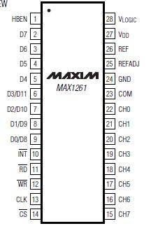
Features: ` 12-Bit Resolution, ±0.5 LSB Linearity
` +3V Single Operation
` User-Adjustable Logic Level (+1.8V to +3.6V)
` Internal +2.5V Reference
` Software-Configurable, Analog Input Multiplexer
8-Channel Single Ended/ 4-Channel Pseudo-Differential (MAX1261)
4-Channel Single Ended/2-Channel Pseudo-Differential (MAX1263)
` Software-Configurable, Unipolar/Bipolar Inputs
` Low Power
1.9mA (250ksps)
1.0mA (100ksps)
400A (10ksps)
2A (Shutdown)
` Internal 3MHz Full-Power Bandwidth Track/Hold
` Byte-Wide Parallel (8 + 4) Interface
` Small Footprint
28-Pin QSOP (MAX1261)
24-Pin QSOP (MAX1263)Application·Industrial Control Systems
·Data Logging
·Energy Management
·Patient Monitoring
·Data-Acquisition Systems
·Touch ScreensPinout Specifications
VDD to GND..............................................................-0.3V to +6V
VLOGIC to GND.........................................................-0.3V to +6V
CH0CH7, COM to GND...............................-0.3V to (VDD + 0.3V)
REF, REFADJ to GND ....................................-0.3V to (VDD + 0.3V)
Digital Inputs to GND ...............................................-0.3V to +6V
Digital Outputs (D0D11, INT) to GND...-0.3V to (VLOGIC + 0.3V)
Continuous Power Dissipation (TA = +70°C)
24-Pin QSOP (derate 9.5mW/°C above +70°C) ............762mW
28-Pin QSOP (derate 8.0mW/°C above +70°C) ............667mW
Operating Temperature Ranges
MAX1261_C_ _/MAX1263_C_ _...........................0°C to +70°C
MAX1261_E_ _/MAX1263_E_ _ .......................-40°C to +85°C
Storage Temperature Range .........................-65°C to +150°C
Lead Temperature (soldering, 10s) ...............................+300°C
Stresses beyond those listed under "Absolute Maximum Ratings" may cause permanent damage to the device. These are stress ratings only, and functional operation of the device at these or any other conditions beyond those indicated in the operational sections of the specifications is not implied. Exposure to absolute maximum rating conditions for extended periods may affect device reliability.
DescriptionThe MAX1261/MAX1263 low-power, 12-bit analog-todigital converters (ADCs) feature a successive-approximation ADC, automatic power-down, fast wake-up (2s), an on-chip clock, +2.5V internal reference, and a high-speed, byte-wide parallel interface. They operate with a single +3V analog supply and feature a VLOGIC pin that allows them to interface directly with a +1.8V to +5.5V digital supply.
Power consumption is only 5.7mW (VDD = VLOGIC) at the maximum sampling rate of 250ksps. Two softwareselectable power-down modes enable the MAX1261/ MAX1263 to be shut down between conversions; accessing the parallel interface returns them to normal operation. Powering down between conversions can cut supply current to under 10A at reduced sampling rates.
Both devices offer software-configurable analog inputs for unipolar/bipolar and single-ended/pseudo-differential operation. In single-ended mode, the MAX1261 has eight input channels and the MAX1263 has four input channels (four and two input channels, respectively, when in pseudo-differential mode).
Excellent dynamic performance and low power, combined with ease of use and small package size, make these converters ideal for battery-powered and dataacquisition applications or for other circuits with demanding power consumption and space requirements.
The MAX1261 is available in a 28-pin QSOP package, while the MAX1263 is available in a 24-pin QSOP. For pin-compatible +5V, 12-bit versions, refer to the MAX1262/MAX1264 data sheet.

 MAX1263 Data Sheet


