MAX12557

Features: ♦ Direct IF Sampling Up to 400MHz♦ Excellent Dynamic Performance74.1dB/72.5dB SNR at fIN = 70MHz/175MHz 83.4dBc/79.5dBc SFDR at fIN = 70MHz/175MHz♦ 3.3V Low-Power Operation 637mW (Differential Clock Mode) 610mW (Single-Ended Clock Mode)♦ Fully Differential or Sing...

product image

MAX12557 Picture
SeekIC No. : 004408686 Detail

MAX12557: Features: ♦ Direct IF Sampling Up to 400MHz♦ Excellent Dynamic Performance74.1dB/72.5dB SNR at fIN = 70MHz/175MHz 83.4dBc/79.5dBc SFDR at fIN = 70MHz/175MHz♦ 3.3V Low-Power Operati...

floor Price/Ceiling Price

Part Number:
MAX12557
Supply Ability:
5000

Price Break

  • Qty
  • 1~5000
  • Unit Price
  • Negotiable
  • Processing time
  • 15 Days
Total Cost: $ 0.00

SeekIC Buyer Protection PLUS - newly updated for 2013!

  • Escrow Protection.
  • Guaranteed refunds.
  • Secure payments.
  • Learn more >>

Month Sales

268 Transactions

Rating

evaluate  (4.8 stars)

Upload time: 2024/11/27

Payment Methods

All payment methods are secure and covered by SeekIC Buyer Protection PLUS.

Notice: When you place an order, your payment is made to SeekIC and not to your seller. SeekIC only pays the seller after confirming you have received your order. We will also never share your payment details with your seller.
Product Details

Description


Features:

♦ Direct IF Sampling Up to 400MHz
♦ Excellent Dynamic Performance
      74.1dB/72.5dB SNR at fIN = 70MHz/175MHz
      83.4dBc/79.5dBc SFDR at fIN = 70MHz/175MHz
♦ 3.3V Low-Power Operation
       637mW (Differential Clock Mode)
       610mW (Single-Ended Clock Mode)
♦ Fully Differential or Single-Ended Analog Input
♦ Adjustable Differential Analog Input Voltage
♦ 750MHz Input Bandwidth
♦ Adjustable, Internal or External, Shared Reference
♦ Differential or Single-Ended Clock
♦ Accepts 25% to 75% Clock Duty Cycle
♦ User-Selectable DIV2 and DIV4 Clock Modes
♦ Power-Down Mode
♦ CMOS Outputs in Two's Complement or Gray Code
♦ Out-of-Range and Data-Valid Indicators
♦ Small, 68-Pin Thin QFN Package
♦ 12-Bit Compatible Version Available (MAX12527)
♦ Evaluation Kit Available (Order MAX12557 EV Kit)


Application

IF and Baseband Communication Receives Cellular, LMDS, Point-to-Point Microwave, MMDS, HFC, WLAN
I/Q Receivers
Ultrasound and Medical Imaging
Portable Instrumentation
Digital Set-Top Boxes
Low-Power Data Acquisition


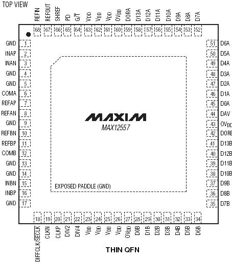
Pinout

  Connection Diagram


Specifications

VDD to GND ................................................................-0.3V to +3.6V
OVDD to GND...............-0.3V to the lower of (VDD + 0.3V) and +3.6V
INAP, INAN to GND .....-0.3V to the lower of (VDD + 0.3V) and +3.6V
INBP, INBN to GND .....-0.3V to the lower of (VDD + 0.3V) and +3.6V
CLKP, CLKN to
GND............................-0.3V to the lower of (VDD + 0.3V) and +3.6V
REFIN, REFOUT
to GND .......................-0.3V to the lower of (VDD + 0.3V) and +3.6V
REFAP, REFAN,
COMA to GND ............-0.3V to the lower of (VDD + 0.3V) and +3.6V
REFBP, REFBN,
COMB to GND ............-0.3V to the lower of (VDD + 0.3V) and +3.6V
DIFFCLK/SECLK, G/T, PD, SHREF, DIV2,
DIV4 to GND ..............-0.3V to the lower of (VDD + 0.3V) and +3.6V
D0AD13A, D0BD13B, DAV,
DORA, DORB to GND......................................-0.3V to (OVDD + 0.3V)
Continuous Power Dissipation (TA = +70°C)
68-Pin Thin QFN 10mm x 10mm x 0.8mm
(derate 70mW/°C above +70°C) .......................................4000mW
Operating Temperature Range................................-40°C to +85°C
Junction Temperature...........................................................+150°C
Storage Temperature Range .................................-65°C to +150°C
Lead Temperature (soldering 10s)........................................+300°C


Description

The MAX12557 is a dual 3.3V, 14-bit analog-to-digital converter (ADC) featuring fully differential wideband track-and-hold (T/H) inputs, driving internal quantizers. The MAX12557 is optimized for low power, small size, and high dynamic performance in intermediate frequency (IF) and baseband sampling applications. This dual ADC operates from a single 3.3V supply, consuming only 610mW while delivering a typical 72.5dB signal-tonoise ratio (SNR) performance at a 175MHz input frequency. The T/H input stages accept single-ended or differential inputs up to 400MHz. In addition to low operating power, the MAX12557 features a 166µW powerdown mode to conserve power during idle periods.

A flexible reference structure allows the MAX12557 to use the internal 2.048V bandgap reference or accept an externally applied reference and allows the reference to be shared between the two ADCs. The reference structure allows the full-scale analog input range to be adjusted from ±0.35V to ±1.15V. The MAX12557 provides a common-mode reference to simplify design and reduce external component count in differential analog input circuits.

The MAX12557 supports either a single-ended or differential input clock. User-selectable divide-by-two (DIV2) and divide-by-four (DIV4) modes allow for design flexibility and help eliminate the negative effects of clock jitter. Wide variations in the clock duty cycle are compensated with the ADC's internal duty-cycle equalizer (DCE).

The MAX12557 features two parallel, 14-bit-wide, CMOS-compatible outputs. The digital output format is pin-selectable to be either two's complement or Gray code. A separate power-supply input for the digital outputs accepts a 1.7V to 3.6V voltage for flexible interfacing with various logic levels. The MAX12557 is available in a 10mm x 10mm x 0.8mm, 68-pin thin QFN package with exposed paddle (EP), and is specified for the extended (-40°C to +85°C) temperature range.

For a 12-bit, pin-compatible version of this ADC, refer to the MAX12527 data sheet.


Customers Who Bought This Item Also Bought

Margin,quality,low-cost products with low minimum orders. Secure your online payments with SeekIC Buyer Protection.
Integrated Circuits (ICs)
Resistors
Potentiometers, Variable Resistors
Tapes, Adhesives
803
RF and RFID
View more