Features: · 210Msps Conversion Rate
· Excellent Low-Noise Characteristics
SNR = 66.6dB at fIN = 100MHz
SNR = 65.5dB at fIN = 200MHz
· Excellent Dynamic Range
SFDR = 81dBc at fIN = 100MHz
SFDR = 79dBc at fIN = 200MHz
· Single 1.8V Supply
· 1.6W Power Dissipation at fSAMPLE = 210Msps and fIN = 10MHz
· On-Chip Track-and-Hold Amplifier
· Internal 1.24V Bandgap Reference
· On-Chip Selectable Divide-by-2 Clock Input
· LVDS Digital Outputs with Data Clock Output
· EV Kit Available (Order MAX1219EVKIT)Application·Cable Modem Termination Systems (CMTS)
·Cable Digital Return Path Transmitters
·Cellular Base-Station Power-Amplifier Linearization
·IF and Baseband Digitization
·ATE and Instrumentation
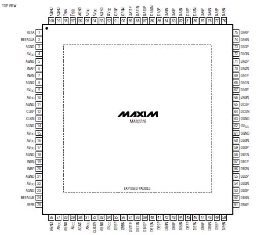
·Radar SystemsPinout Specifications
AVCC to AGND ....................................................-0.3V to +2.1V
OVCC to OGND ...................................................-0.3V to +2.1V
OVCC to AVCC ....................................................-0.3V to +0.3V
OGND to AGND ...................................................-0.3V to +0.3V
CLKP, CLKN, INAP, INAN, INBP,
INBN to AGND .......................................-0.3V to (AVCC + 0.3V)
CLKDIV, T/BA, T/BB to AGND ..................-0.3V to (AVCC + 0.3V)
REFA, REFADJA, REFB, REFADJB
to AGND.................................................-0.3V to (AVCC + 0.3V)
DCOP, DCON, DA0PDA11P, DA0NDA11N,
DB0PDB11P, DB0NDB11N, ORAP, ORAN,
ORBP, ORBN to OGND...........................-0.3V to (OVCC + 0.3V)
Current into any Pin.........................................................50mA
ESD Voltage on INAP, INAN, INBP, INBN
(Human Body Model).....................................................±750V
ESD Voltage on All Other Pins (Human Body Model)....±2000V
Continuous Power Dissipation (TA = +70°C)
100-Pin TQFP (derate 37mW/°C above +70°C).......2963mW
Operating Temperature Range .....................-40°C to +85°C
Storage Temperature Range ......................-65°C to +150°C
Junction Temperature..................................................+150°C
Lead Temperature (soldering, 10s) ............................+300°C
Stresses beyond those listed under "Absolute Maximum Ratings" may cause permanent damage to the device. These are stress ratings only, and functional operation of the device at these or any other conditions beyond those indicated in the operational sections of the specifications is not implied. Exposure to absolute maximum rating conditions for extended periods may affect device reliability.
DescriptionThe MAX1219 dual, monolithic, 12-bit, 210Msps analogto- digital converter (ADC) provides outstanding dynamic performance up to a 250MHz input frequency. The device operates with conversion rates up to 210Msps while consuming only 800mW per channel.
At 210Msps and an input frequency of 200MHz, the MAX1219 achieves a 79dBc spurious-free dynamic range (SFDR) with excellent 65.5dB signal-to-noise ratio (SNR) at 200MHz. The SNR remains flat (within 3dB) for input tones up to 250MHz. This makes the MAX1219 ideal for wideband applications such as communications receivers, cable head-end receivers, and power-amplifier predistortion in cellular base-station transceivers. The MAX1219 operates from a single 1.8V power supply. The analog inputs of each channel are designed for AC-coupled, differential or single-ended operation.
The ADC also features a selectable on-chip divide-by-2 clock circuit that accepts clock frequencies as high as 420MHz and reduces the phase noise of the input clock source. A low-voltage differential signal (LVDS) sampling clock is recommended for best performance. The converter's digital outputs are LVDS compatible and the data format can be selected to be either two's complement or offset binary.
The MAX1219 is available in a 100-pin TQFP package with exposed paddle and is specified over the extended (-40°C to +85°C) temperature range. Refer to the MAX1218 (170Msps) and the MAX1217 (125Msps) data sheets for lower speed, pin-compatible devices.

 MAX1219 Data Sheet


