Features: · 210Msps Conversion Rate
· Low Noise Floor of -67.6dBFS
· Excellent Low-Noise Characteristics
SNR = 65.6dB at fIN = 100MHz
SNR = 65dB at fIN = 250MHz
· Excellent Dynamic Range
SFDR = 74.2dBc at fIN = 100MHz
SFDR = 77.2dBc at fIN = 250MHz
· 59.5dB NPR for fNOTCH = 28.8MHz and a Noise Bandwidth of 50MHz
· Single 1.8V Supply
· 820mW Power Dissipation at fSAMPLE = 210MHz and fIN = 100MHz
· On-Chip Track-and-Hold Amplifier
· Internal 1.23V-Bandgap Reference
· On-Chip Selectable Divide-by-2 Clock Input
· LVDS Digital Outputs with Data Clock Output
· MAX1214 EV Kit Available
Application·Base-Station Power-Amplifier Linearization
·Cable-Head End Receivers
·Wireless and Wired Broadband Communication
·Communications Test Equipment
·Radar and Satellite SubsystemsPinout Specifications
AVCC to AGND ..................................................-0.3V to +2.1V
OVCC to OGND .................................................-0.3V to +2.1V
AVCC to OVCC ..................................................-0.3V to +2.1V
AGND to OGND .................................................-0.3V to +0.3V
INP, INN to AGND..................................-0.3V to (AVCC + 0.3V)
All Digital Inputs to AGND......................-0.3V to (AVCC + 0.3V)
REFIO, REFADJ to AGND ........................-0.3V to (AVCC + 0.3V)
All Digital Outputs to OGND ..................-0.3V to (OVCC + 0.3V)
ESD on All Pins (Human Body Model) ...........................±2000V
Thermal Resistance
jC ...............................................................................0.8°C/W
jA.................................................................................35°C/W
Operating Temperature Range .......................-40°C to +85°C
Junction Temperature ...................................................+150°C
Storage Temperature Range .........................-60°C to +150°C
Maximum Current into Any Pin ........................................±50mA
Lead Temperature (soldering,10s) ................................+300°C
Stresses beyond those listed under "Absolute Maximum Ratings" may cause permanent damage to the device. These are stress ratings only, and functional operation of the device at these or any other conditions beyond those indicated in the operational sections of the specifications is not implied. Exposure to absolute maximum rating conditions for extended periods may affect device reliability.
DescriptionThe MAX1214 is a monolithic, 12-bit, 210Msps analogto- digital converter (ADC) optimized for outstanding dynamic performance at high-IF frequencies up to 300MHz. The product operates with conversion rates up to 210Msps while consuming only 820mW.
At 210Msps and an input frequency up to 250MHz, the MAX1214 achieves a spurious-free dynamic range (SFDR) of 77.2dBc. Its excellent signal-to-noise ratio (SNR) of 66dB at 10MHz remains flat (within 2dB) for input tones up to 300MHz. This ADC yields an excellent low noise floor of -67.6dBFS, which makes it ideal for wideband applications such as cable-head end receivers and power-amplifier predistortion in cellular base-station transceivers.
The MAX1214 requires a single 1.8V supply. The analog input is designed for either differential or single-ended operation and can be AC- or DC-coupled. The ADC also features a selectable on-chip divide-by-2 clock circuit, which allows the user to apply clock frequencies as high as 340MHz. This helps to reduce the phase noise of the input clock source. A low-voltage differential signal (LVDS) sampling clock is recommended for best performance. The converter's digital outputs are LVDS compatible and the data format can be selected to be either two's complement or offset binary.
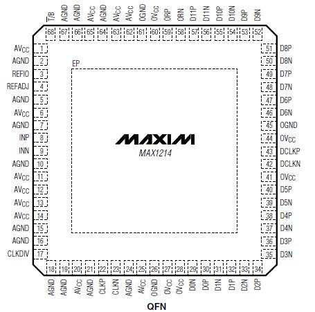
The MAX1214 is available in a 68-pin QFN package with exposed paddle (EP) and is specified over the industrial (-40°C to +85°C) temperature range.
See the Pin-Compatible Versions table for a complete selection of 8-bit, 10-bit, and 12-bit high-speed DACs in this family.

 MAX1214 Data Sheet


