Packaging
:
Number of Converters
: 2
Mounting Style
: SMD/SMT
Supply Voltage - Max
: 3.6 V
Supply Voltage - Min
: 2.7 V
Number of ADC Inputs
: 2
Input Type
: Voltage
Maximum Operating Temperature
: + 85 C
Resolution
: 8 bit
Interface Type
: Parallel
Architecture
: Pipelined
Conversion Rate
: 45 MSPs
Maximum Power Dissipation
: 1667 mW
SNR
: 48.5 dB
Voltage Reference
: 1.024 V
Package / Case
: TQFN EP
Features: Ultra-Low Power 57mW (Normal Operation: 45Msps) 0.3W (Shutdown Mode)
Excellent Dynamic Performance 48.5dB/48.3dB SNR at fIN = 5.5MHz/100MHz 70dBc/68dBc SFDR at fIN = 5.5MHz/100MHz
2.7V to 3.6V Single Analog Supply
1.8V to 3.6V TTL/CMOS-Compatible Digital Outputs
Fully Differential or Single-Ended Analog Inputs
Internal/External Reference Option
Multiplexed CMOS-Compatible Tri-State Outputs
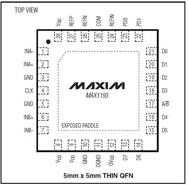
28-Pin Thin QFN Package
Evaluation Kit Available (Order MAX1193EVKIT)ApplicationUltrasound and Medical Imaging
IQ Baseband Sampling
Battery-Powered Portable Instruments
Low-Power Video
WLAN, Mobile DSL, WLL ReceiverPinout Specifications
VDD, OVDD to GND ......................................................................................................................-0.3V to +3.6V
OGND to GND................................................................................................................................-0.3V to +0.3V
INA+, INA-, INB+, INB- to GND ..........................................................................................-0.3V to (VDD + 0.3V)
CLK, REFIN, REFP, REFN, COM to GND................................................................................-0.3V to (VDD + 0.3V)
PD0, PD1 to OGND ..........................................................................................................-0.3V to (OVDD + 0.3V)
Digital Outputs to OGND...................................................................................................-0.3V to (OVDD + 0.3V
Continuous Power Dissipation (TA = +70°C)28-Pin Thin QFN (derated 20.8mW/°C above +70°C) ..1667mW
Operating Temperature Range ...............................................................................................-40°C to +85°C
Junction Temperature............................................................................................................................+150°C
Storage Temperature Range ................................................................................................ -65°C to +150°C
Lead Temperature (soldering, 10s) .......................................................................................................+300°C
DescriptionThe MAX1193 is an ultra-low-power, dual, 8-bit, 45Msps analog-to-digital converter (ADC). The device features two fully differential wideband track-and-hold (T/H) inputs. These inputs have a 440MHz bandwidth and accept fully differential or single-ended signals. The MAX1193 delivers a typical signal-to-noise and distortion(SINAD) of 48.5dB at an input frequency of 5.5MHz and a sampling rate of 45Msps while consuming only 57mW. This ADC operates from a 2.7V to 3.6V analog power supply. A separate 1.8V to 3.6V supply powers the digital output driver. In addition to ultra-low operating power, the MAX1193 features three powerdown modes to conserve power during idle periods. Excellent dynamic performance, ultra-low power, and small size make the MAX1193 ideal for applications in imaging, instrumentation, and digital communications.
An internal 1.024V precision bandgap reference sets the full-scale range of the ADC to ±0.512V. A flexible reference structure allows the MAX1193 to use its internal
reference or accept an externally applied reference for applications requiring increased accuracy.
The MAX1193 features parallel, multiplexed, CMOScompatible tri-state outputs. The digital output format is offset binary. A separate digital power input accepts a voltage from 1.8V to 3.6V for flexible interfacing to different logic levels. The MAX1193 is available in a 5mm* 5mm, 28-pin thin QFN package, and is specified for the extended industrial (-40°C to +85°C) temperature range.
For higher sampling frequency applications, refer to the MAX1195MAX1198 dual 8-bit ADCs. Pin-compatible versions of the MAX1193 are also available. Refer to the MAX1191 data sheet for 7.5Msps, and the MAX1192 data sheet for 22Msps.

 MAX1193ETI-T Data Sheet


