Features: Ultra-Low Power12mW (Normal Operation: 7.5Msps)0.3PAW (Shutdown Mode)Excellent Dynamic Performance48.7dB SNR at fIN= 1.875MHz69dBc SFDR at fIN= 1.875MHz2.7V to 3.6V Single Analog Supply1.8V to 3.6V TTL/CMOS-Compatible Digital OutputsFully Differential or Single-Ended Analog Inputs nterna...
MAX1191: Features: Ultra-Low Power12mW (Normal Operation: 7.5Msps)0.3PAW (Shutdown Mode)Excellent Dynamic Performance48.7dB SNR at fIN= 1.875MHz69dBc SFDR at fIN= 1.875MHz2.7V to 3.6V Single Analog Supply1.8...
SeekIC Buyer Protection PLUS - newly updated for 2013!
268 Transactions
All payment methods are secure and covered by SeekIC Buyer Protection PLUS.
Ultra-Low Power
12mW (Normal Operation: 7.5Msps)
0.3PAW (Shutdown Mode)
Excellent Dynamic Performance
48.7dB SNR at fIN= 1.875MHz
69dBc SFDR at fIN= 1.875MHz
2.7V to 3.6V Single Analog Supply
1.8V to 3.6V TTL/CMOS-Compatible Digital Outputs
Fully Differential or Single-Ended Analog Inputs nternal/External Reference Option
Multiplexed CMOS-Compatible Tri-State Outputs 28-Pin Thin QFN Package
Evaluation Kit Available (Order MAX1193EVKIT)
The MAX1191 is an ultra-low-power, dual, 8-bit, 7.5Msps analog-to-digital converter (ADC). The device features two fully differential wideband track-and-hold (T/H) inputs. These inputs have a 440MHz bandwidth and accept fully differential or single-ended signals. The MAX1191 delivers a typical signal-to-noise and distortion (SINAD) of 48.6dB at an input frequency of 1.875MHz and a sampling rate of 7.5Msps while consuming only 12mW. This ADC operates from a 2.7V to 3.6V analog power supply. A separate 1.8V to 3.6V supply powers the digital output driver. In addition to ultra-low operating power, the MAX1191 features three power-down modes to conserve power during idle periods. Excellent dynamic performance, ultra-low power, and small size make the MAX1191 ideal for applications in imaging, instrumentation, and digital communications
An internal 1.024V precision bandgap reference sets the full-scale range of the ADC to ±0.512V. A flexible reference structure allows the device to use its internal reference or accept an externally applied reference for applications requiring increased accuracy.
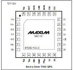
The MAX1191 features parallel, multiplexed, CMOScompatible tri-state outputs. The digital output format is offset binary. A separate digital power input accepts a voltage from 1.8V to 3.6V for flexible interfacing to different logic levels. The MAX1191 is available in a 5mm * 5mm, 28-pin thin QFN package, and is specified for the extended industrial (-40°C to +85°C) temperature range.
For higher sampling frequency applications, refer to the MAX1195MAX1198 dual 8-bit ADCs. Pin-compatible versions of the MAX1191 are also available. Refer to the MAX1192 data sheet for 22Msps, and the MAX1193 data sheet for 45Msps.