Features: Single 3.3V Operation
Excellent Dynamic Performance 57dB SINAD at fIN = 60MHz 64dBc SFDR at fIN = 60MHz
-71dBc Interchannel Crosstalk at fIN = 60MHz
Low Power 492mW (Normal Operation) 10mW (Sleep Mode) 3.3µW (Shutdown Mode)
0.08dB Gain and 0.8° Phase Matching
Wide ±1VP-P Differential Analog Input Voltage Range
400MHz -3dB Input Bandwidth
On-Chip 2.048V Precision Bandgap Reference
User-Selectable Output Format-Two's Complement or Offset Binary
Pin-Compatible, Lower-Speed, 10-Bit and 8-Bit Versions Available
ApplicationBaseband I/Q Sampling
Multichannel IF Sampling
Ultrasound and Medical Imaging
Battery-Powered Instrumentation
WLAN, WWAN, WLL, MMDS Modems
Set-Top Boxes
VSAT Terminals
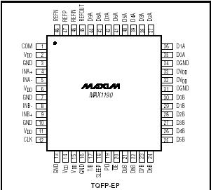
Pinout Specifications
VDD, OVDD to GND ...............................................-0.3V to +3.6V
OGND to GND.......................................................-0.3V to +0.3V
INA+, INA-, INB+, INB- to GND ...............................-0.3V to VDD
REFIN, REFOUT, REFP, REFN, COM, CLK to GND....-0.3V to (VDD + 0.3V)
OE, PD, SLEEP, T/B, D9AD0A, D9BD0B to OGND ...-0.3V to (OVDD + 0.3V)
Continuous Power Dissipation (TA = +70°C)
48-Pin TQFP (derate 12.5mW/°C above +70°C)........1000mW
Operating Temperature Range ...........................-40°C to +85°C
Junction Temperature......................................................+150°C
Storage Temperature Range .............................-60°C to +150°C
Lead Temperature (soldering, 10s) .................................+300°C
DescriptionThe MAX1190 is a 3.3V, dual 10-bit analog-to-digital converter (ADC) featuring fully differential wideband trackand- hold (T/H) inputs, driving two ADCs. The MAX1190 is optimized for low power, small size, and high-dynamic performance for applications in imaging, instrumentation, and digital communications. This ADC operates from a single 2.8V to 3.6V supply, consuming only 492mW while delivering a typical signal-to-noise and distortion (SINAD) of 57dB at an input frequency of 60MHz and a sampling rate of 120Msps. The T/H driven input stages incorporate 400MHz (-3dB) input amplifiers. The converters can also be operated with single-ended inputs. In addition to low operating power, the device features a 3mA sleep mode, as well as a 1µA power-down mode to conserve power during idle periods.
An internal 2.048V precision bandgap reference sets the full-scale range of the ADC. A flexible reference structure allows the use of this internal or an externally applied reference, if desired, for applications requiring increased accuracy or a different input voltage range.
The MAX1190 features parallel, CMOS-compatible threestate outputs. The digital output format can be set to two's complement or straight offset binary through a single control pin. The device provides for a separate output power supply of 1.7V to 3.6V for flexible interfacing with various logic families. The MAX1190 is available in a 7mm ✕ 7mm, 48 pin TQFP-EP package, and is specified for the extended industrial (-40°C to +85°C) temperature range.
Pin-compatible lower speed versions of the MAX1190 are also available. Refer to the MAX1180MAX1184 data sheets for 105Msps/80Msps/65Msps/40Msps. In addition to these speed grades, this family includes two multiplexed output versions (MAX1185/MAX1186 for 20Msps/40Msps), for which digital data is presented time-interleaved and on a single, parallel 10-bit output port.
For lower speed, pin-compatible, 8-bit versions of the MAX1190, refer to the MAX1195MAX1198 data sheets.

 MAX1190 Data Sheet


