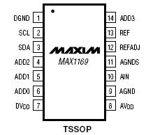
Features: High-Speed I2C-Compatible Serial Interface
400kHz Fast Mode
1.7MHz High-Speed Mode
+4.75V to +5.25V Single Supply
+2.7V to +5.5V Adjustable Logic Level
Internal +4.096V Reference
External Reference: 1V to AVDD
Internal 4MHz Conversion Clock
58.6ksps Sampling Rate
AutoShutdown Between Conversions
Low Power
5.0mW at 58.6ksps
4.2mW at 50ksps
2.0mW at 10ksps
0.23mW at 1ksps
3W in Shutdown
Small 14-Pin TSSOP PackageApplicationHand-Held Portable Applications
Medical Instruments
Battery-Powered Test Equipment
Solar-Powered Remote Systems
Received-Signal-Strength Indicators
System SupervisionPinout SpecificationsAVDD to AGND .........................................................-0.3V to +6V
DVDD to DGND.........................................................-0.3V to +6V
AGND to DGND......................................................-0.3V to +0.3V
AGNDS to AGND....................................................-0.3V to +0.3V
AIN, REF, REFADJ to AGND........................-0.3V to (AVDD + 0.3V)
SCL, SDA, ADD_ to DGND.........................................-0.3V to +6V
Maximum Current into Any Pin............................................50mA
Continuous Power Dissipation (TA = +70°C)
14-Pin TSSOP (derate 9.1mW/°C above +70°C) .......727mW
Operating Temperature Ranges
MAX1169_CUD ................................................0°C to +70°C
MAX1169_EUD .............................................-40°C to +85°C
Storage Temperature Range ........................-65°C to +150°C
Junction Temperature...................................................+150°C
Lead Temperature (soldering, 10s) ..............................+300°CDescriptionThe MAX1169 is a low-power, 16-bit successiveapproximation analog-to-digital converter (ADC). The device features automatic power down, an on-chip 4MHz clock, a +4.096V internal reference, and an I
2C-compatible 2-wire serial interface capable of both fast and high speed modes.
The MAX1169 operates from a single supply and consumes 5mW at the maximum conversion rate of 58.6ksps. AutoShutdown™ powers down the device between conversions, reducing supply current to less than 50A at a 1ksps throughput rate. The option of a separate digital supply voltage allows direct interfacing with +2.7V to +5.5V digital logic.
The MAX1169 performs a unipolar conversion on its single analog input using its internal 4MHz clock. The full-scale analog input range is determined by the internal reference or by an externally applied reference voltage ranging from 1V to AV
DD.
The four address select inputs (ADD0 to ADD3) allow up to 16 MAX1169 devices on the same bus.
The MAX1169 is packaged in a 14-pin TSSOP and offers both commercial and extended temperature ranges. Refer to the MAX1069 data sheet for a 14-bit device in a pin-compatible package.

 MAX1169 Data Sheet


