MAX1126

Features: · Four ADC Channels with Serial LVDS/SLVS Outputs· Excellent Dynamic Performance 69.9dB SNR at fIN = 5.3MHz 93.7dBc SFDR at fIN = 5.3MHz -90dB Channel Isolation· Ultra-Low Power 135mW per Channel (Normal Operation) 1.5mW Total (Shutdown Mode)· Accepts 20% to 80% Clock Duty Cycle· Self-Al...

product image

MAX1126 Picture
SeekIC No. : 004408514 Detail

MAX1126: Features: · Four ADC Channels with Serial LVDS/SLVS Outputs· Excellent Dynamic Performance 69.9dB SNR at fIN = 5.3MHz 93.7dBc SFDR at fIN = 5.3MHz -90dB Channel Isolation· Ultra-Low Power 135mW per ...

floor Price/Ceiling Price

Part Number:
MAX1126
Supply Ability:
5000

Price Break

  • Qty
  • 1~5000
  • Unit Price
  • Negotiable
  • Processing time
  • 15 Days
Total Cost: $ 0.00

SeekIC Buyer Protection PLUS - newly updated for 2013!

  • Escrow Protection.
  • Guaranteed refunds.
  • Secure payments.
  • Learn more >>

Month Sales

268 Transactions

Rating

evaluate  (4.8 stars)

Upload time: 2024/11/27

Payment Methods

All payment methods are secure and covered by SeekIC Buyer Protection PLUS.

Notice: When you place an order, your payment is made to SeekIC and not to your seller. SeekIC only pays the seller after confirming you have received your order. We will also never share your payment details with your seller.
Product Details

Description


Features:

· Four ADC Channels with Serial LVDS/SLVS
    Outputs
· Excellent Dynamic Performance
    69.9dB SNR at fIN = 5.3MHz
    93.7dBc SFDR at fIN = 5.3MHz
    -90dB Channel Isolation
· Ultra-Low Power
    135mW per Channel (Normal Operation)
    1.5mW Total (Shutdown Mode)
· Accepts 20% to 80% Clock Duty Cycle
· Self-Aligning Data-Clock to Data-Output Interface
· Fully Differential Analog Inputs
· Wide ±1.4VP-P Differential Input Voltage Range
· Internal/External Reference Option
· Test Mode for Digital Signal Integrity
· LVDS Outputs Support Up to 30in FR-4 Backplane
    Connections
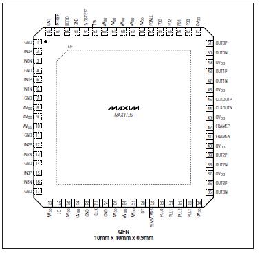
· Small, 68-Pin QFN with Exposed Paddle
· Evaluation Kit Available (MAX1127EVKIT)


Application

Ultrasound and Medical Imaging
Positron Emission Tomography (PET) Imaging
Multichannel Communication Systems
Instrumentation


Pinout

  Connection Diagram


Specifications

AVDD to GND........................................................-0.3V to +2.0V
CVDD to GND .......................................................-0.3V to +3.6V
OVDD to GND .......................................................-0.3V to +2.0V
IN_P, IN_N to GND...................................-0.3V to (AVDD + 0.3V)
CLK to GND..............................................-0.3V to (CVDD + 0.3V)
OUT_P, OUT_N, FRAME_,
CLKOUT_ to GND.....................................-0.3V to (OVDD + 0.3V)
DT, SLVS/LVDS to GND.............................-0.3V to (AVDD + 0.3V)
PLL0, PLL1, PLL2, PLL3 to GND ...............-0.3V to (AVDD + 0.3V)
PD0, PD1, PD2, PD3, PDALL to GND.........-0.3V to (AVDD + 0.3V)
T/B, LVDSTEST to GND ............................-0.3V to (AVDD + 0.3V)
REFIO, NTREF to GND..............................-0.3V to (AVDD + 0.3V)
I.C. to GND..............................................-0.3V to (AVDD + 0.3V)
Continuous Power Dissipation (TA = +70)
68-Pin QFN 10mm x 10mm x 0.9mm
(derated 41.7mW/above +70).............................3333.3mW
Operating Temperature Range ...........................-40 to +85
Maximum Junction Temperature .....................................+150
Storage Temperature Range ............................-65 to +150
Lead Temperature Range (soldering, 10s)......................+300


Description

The MAX1126 quad, 12-bit analog-to-digital converter (ADC) features fully differential inputs, a pipelined architecture, and digital error correction. This ADC is
optimized for low-power, high-dynamic performance for medical imaging, communications, and instrumentation applications. The MAX1126 operates from a 1.7V to 1.9V single supply and consumes only 563mW while delivering a 69.9dB signal-to-noise ratio (SNR) at a 5.3MHz input frequency. In addition to low operating power, the MAX1126 features an 813A power-down mode for idle periods.

An internal 1.24V precision bandgap reference sets the ADC's full-scale range. A flexible reference structure allows the use of an external reference for applications requiring increased accuracy or a different input voltage range.

A single-ended clock controls the conversion process.

An internal duty-cycle equalizer allows for wide variations in input-clock duty cycle. An on-chip phaselocked loop (PLL) generates the high-speed serial low-voltage differential signaling (LVDS) clock.

The MAX1126 provides serial LVDS outputs for data, clock, and frame alignment signals. The output data is presented in two's complement or binary format.
Refer to the MAX1127 data sheet for a pin-compatible 65Msps version of the MAX1126.

The MAX1126 is available in a small, 10mm x 10mm x 0.9mm, 68-pin QFN package with exposed paddle and is specified for the extended industrial (-40to +85) temperature range.


Customers Who Bought This Item Also Bought

Margin,quality,low-cost products with low minimum orders. Secure your online payments with SeekIC Buyer Protection.
Optoelectronics
Discrete Semiconductor Products
Inductors, Coils, Chokes
Sensors, Transducers
View more