MAX1121

Features: · 250Msps Conversion Rate· SNR = 48.8dB/48.7dB at fIN = 100MHz/500MHz· SFDR = 68dBc/63.8dBc at fIN = 100MHz/500MHz· Single 1.8V Supply· 477mW Power Dissipation at 250Msps· On-Chip Track-and-Hold and Internal Reference· On-Chip Selectable Divide-by-2 Clock Input· LVDS Digital Outputs with...

product image

MAX1121 Picture
SeekIC No. : 004408502 Detail

MAX1121: Features: · 250Msps Conversion Rate· SNR = 48.8dB/48.7dB at fIN = 100MHz/500MHz· SFDR = 68dBc/63.8dBc at fIN = 100MHz/500MHz· Single 1.8V Supply· 477mW Power Dissipation at 250Msps· On-Chip Track-an...

floor Price/Ceiling Price

Part Number:
MAX1121
Supply Ability:
5000

Price Break

  • Qty
  • 1~5000
  • Unit Price
  • Negotiable
  • Processing time
  • 15 Days
Total Cost: $ 0.00

SeekIC Buyer Protection PLUS - newly updated for 2013!

  • Escrow Protection.
  • Guaranteed refunds.
  • Secure payments.
  • Learn more >>

Month Sales

268 Transactions

Rating

evaluate  (4.8 stars)

Upload time: 2024/11/27

Payment Methods

All payment methods are secure and covered by SeekIC Buyer Protection PLUS.

Notice: When you place an order, your payment is made to SeekIC and not to your seller. SeekIC only pays the seller after confirming you have received your order. We will also never share your payment details with your seller.
Product Details

Description


Features:

· 250Msps Conversion Rate
· SNR = 48.8dB/48.7dB at fIN = 100MHz/500MHz
· SFDR = 68dBc/63.8dBc at fIN = 100MHz/500MHz
· Single 1.8V Supply
· 477mW Power Dissipation at 250Msps
· On-Chip Track-and-Hold and Internal Reference
· On-Chip Selectable Divide-by-2 Clock Input
· LVDS Digital Outputs with Data Clock Output
· Evaluation Kit Available (Order MAX1124EVKIT)


Application

Wireless and Wired Broadband Communication
Digital Oscilloscopes
Digital Predistortion Receivers
Communications Test Equipment
Radar and Satellite Subsystems Antenna Array
Processing
Instrumentation


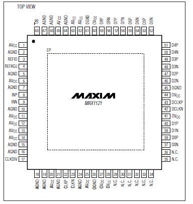
Pinout

  Connection Diagram


Specifications

AVCC to AGND ......................................................-0.3V to +2.1V
OVCC to OGND .....................................................-0.3V to +2.1V
AVCC to OVCC .......................................................-0.3V to +2.1V
AGND to OGND ....................................................-0.3V to +0.3V
Analog Inputs to AGND ...........................-0.3V to (AVCC + 0.3V)
Digital Inputs to AGND.............................-0.3V to (AVCC + 0.3V)
REF, REFADJ to AGND............................-0.3V to (AVCC + 0.3V)
Digital Outputs to OGND.........................-0.3V to (OVCC + 0.3V)
ESD on All Pins (Human Body Model).............................±2000V
Continuous Power Dissipation (TA = +70)
68-Pin QFN (derate 41.7mW/ above +70) .........3333mW
Operating Temperature Range ...........................-40 to +85
Junction Temperature......................................................+150
Storage Temperature Range .............................-60 to +150
Lead Temperature (soldering, 10s) .................................+300
Maximum Current into Any Pin............................................50mA


Description

The MAX1121 is a monolithic 8-bit, 250Msps analog-todigital converter (ADC) optimized for outstanding dynamic performance at high IF frequencies up to
500MHz. The product operates with conversion rates of up to 250Msps while consuming only 477mW.

At 250Msps and an input frequency of 100MHz, the MAX1121 achieves a spurious-free dynamic range (SFDR) of 68dBc. Its excellent signal-to-noise ratio (SNR) of 48.9dB at 10MHz remains flat (within 0.5dB) for input tones up to 500MHz. This makes the MAX1121 ideal for wideband applications such as digital predistortion in cellular base-station transceiver systems.

The MAX1121 requires a single 1.8V supply. The analog input is designed for either differential or singleended operation and can be AC- or DC-coupled. The ADC also features a selectable on-chip divide-by-2 clock circuit, which allows the user to apply clock frequencies as high as 500MHz. This helps to reduce the
phase noise of the input clock source. A differential LVDS sampling clock is recommended for best performance. The converter's digital outputs are LVDS compatible, and the data format can be selected to be either two's complement or offset binary.

The MAX1121 is available in a 68-pin QFN with exposed paddle (EP) and is specified over the industrial (-40 to +85) temperature range.

For pin-compatible, higher resolution versions of the device, refer to the MAX1122 (170Msps), the MAX1123 (210Msps), and the MAX1124 (250Msps) data sheets.


Customers Who Bought This Item Also Bought

Margin,quality,low-cost products with low minimum orders. Secure your online payments with SeekIC Buyer Protection.
Resistors
Audio Products
Circuit Protection
Power Supplies - Board Mount
Memory Cards, Modules
Batteries, Chargers, Holders
View more