Features: ·1.5Gsps Conversion Rate
· 2.2GHz Full-Power Analog Input Bandwidth
· 7.5 Effective Bits at fIN = 750MHz (Nyquist Frequency)
· ±0.25LSB INL and DNL
· 50½ Differential Analog Inputs
· ±250mV Input Signal Range
· On-Chip, +2.5V Precision Bandgap Voltage Reference
· Latched, Differential PECL Digital Outputs
· Selectable 8:16 Demultiplexer
· Internal Demux Reset Input with Reset Output
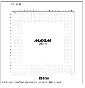
· 192-Contact ESBGA Package
· Pin Compatible with MAX104 (1Gsps) and MAX106 (600Msps)ApplicationDigital RF/IF Signal Processing
Direct RF Downconversion
High-Speed Data Acquisition
Digital Oscilloscopes
High-Energy Physics
Radar/ECM Systems
ATE SystemsPinout Specifications
VCCA to GNDA.................................................................-0.3V to +6V
VCCD to GNDD.................................................................-0.3V to +6V
VCCI to GNDI...................................................................-0.3V to +6V
VCCO to GNDD.................................................-0.3V to (VCCD + 0.3V)
AUXEN1, AUXEN2 to GND ................................-0.3V to (VCCD + 0.3V)
VEE to GNDI................................................. ...................-6V to +0.3V
Between GNDs..............................................................-0.3V to +0.3V
VCCA to VCCD ..............................................................-0.3V to +0.3V
VCCA to VCCI................................................................-0.3V to +0.3V
PECL Digital Output Current .......................................................50mA
REFIN to GNDR............................................................... (VCCI + 0.3V)
REFOUT Current .........................................................+100A to -5mA
ICONST, IPTAT to GNDI .................................................-0.3V to +1.0V
TTL/CMOS Control Inputs
(DEMUXEN, DIVSELECT) .......................................3V to (VCCD + 0.3V)
RSTIN+, RSTIN- ................................................-0.3V to (VCCO + 0.3V)
VOSADJ Adjust Input .........................................-0.3V to (VCCI + 0.3V)
CLK+ to CLK- Voltage Difference....................................................±3V
CLK+, CLK-.................................................(VEE - 0.3V) to (GNDD + 1V)
CLKCOM.......................................... ..........(VEE - 0.3V) to (GNDD + 1V)
VIN+ to VIN- Voltage Difference .....................................................±2V
VIN+, VIN- to GNDI..........................................................................±2V
Continuous Power Dissipation (TA = +70°C)
192-Contact ESBGA (derate 61mW/°C above +70°C) ................4.88W
(with heatsink and 200 LFM airflow,
derate 106mW/°C above +70°C) ...............................................8.48W
Operating Temperature Range
MAX108CHC......................................................................0°C to +70°C
Operating Junction Temperature.................................................+150°C
Storage Temperature Range.......................................-65°C to +150°C
Stresses beyond those listed under "Absolute Maximum Ratings" may cause permanent damage to the device. These are stress ratings only, and func
tional operation of the device at these or any other conditions beyond those indicated in the operational sections of the specifications is not implied. Exp
osure to absolute maximum rating conditions for extended periods may affect device reliability.
DescriptionThe MAX108 PECL-compatible, 1.5Gsps, 8-bit analogto- digital converter (ADC) allows accurate digitizing of analog signals with bandwidths to 2.2GHz. Fabricated on Maxim's proprietary advanced GST-2 bipolar process, the MAX108 integrates a high-performance track/hold (T/H) amplifier and a quantizer on a single monolithic die.
The innovative design of the internal T/H, which has an exceptionally wide 2.2GHz full-power input bandwidth, results in high performance (typically 7.5 effective bits) at the Nyquist frequency. A fully differential comparator design and decoding circuitry reduce out-of-sequence code errors (thermometer bubbles or sparkle codes) and provide excellent metastable performance. Unlike other ADCs that can have errors resulting in false fullor zero-scale outputs, the MAX108 limits the error magnitude to 1LSB.
The analog input is designed for either differential or single-ended use with a ±250mV input voltage range. Dual, differential, positive-referenced emitter-coupled logic (PECL)-compatible output data paths ensure easy interfacing and include an 8:16 demultiplexer feature that reduces output data rates to one-half the sampling clock rate. The PECL outputs can be operated from any supply between +3V to +5V for compatibility with +3.3V or +5V referenced systems. Control inputs are provided for interleaving additional MAX108 devices to increase the effective system sampling rate.
The MAX108 is packaged in a 25mm x 25mm, 192-contact Enhanced Super Ball-Grid Array (ESBGA™) and is specified over the commercial (0°C to +70°C) temperature range. For pin-compatible, lower speed versions of the MAX108, see the MAX104 (1Gsps) and the MAX106 (600Msps) data sheets.

 MAX108 Data Sheet


