Features: ` 10-Bit, 300ksps ADC
Analog Multiplexer with True-Differential Track/Hold (T/H)
8 Single-Ended Channels or 4 Differential Channels (Unipolar or Bipolar)
4 Single-Ended Channels or 2 Differential Channels (Unipolar or Bipolar)
Excellent Accuracy: ±0.5 LSB INL, ±0.5 LSB DNL, No Missing Codes Over Temperature
` 10-Bit, Quad, 2s Settling DAC
Ultra-Low-Glitch Energy (4nV•s)
Power-Up Options from Zero Scale or Full Scale
Excellent Accuracy: ±0.5 LSB INL
` Internal Reference or External Single-Ended/
Differential Reference
Internal Reference Voltage 2.5V or 4.096V
` Internal ±1°C Accurate Temperature Sensor
` On-Chip FIFO Capable of Storing 16 ADC Conversion Results and One Temperature Result
` On-Chip Channel-Scan Mode and Internal Data-Averaging Features
` Analog Single-Supply Operation +2.7V to +3.6V or +4.75V to +5.25V
` 25MHz, SPI/QSPI/MICROWIRE Serial Interface
` AutoShutdown Between Conversions
` Low-Power ADC
2.5mA at 300ksps
22A at 1ksps
0.2A at Shutdown
` Low-Power DAC: 1.5A
` Evaluation Kit Available (Order MAX1258EVKIT)
Application·Closed-Loop Controls for Optical Components and Base Stations
·System Supervision and Control
·Data-Acquisition SystemsPinout Specifications
AVDD to AGND .........................................................-0.3V to +6V
DGND to AGND.....................................................-0.3V to +0.3V
DVDD to AVDD .....................................................-3.0V to +0.3V
Digital Inputs to DGND............................................-0.3V to +6V
Digital Outputs to DGND .........................-0.3V to (DVDD + 0.3V)
Analog Inputs, Analog Outputs and REF_
to AGND..................................................-0.3V to (AVDD + 0.3V)
Maximum Current into Any Pin (except AGND, DGND, AVDD,
DVDD, and OUT_) ..............................................................50mA
Maximum Current into OUT_.............................................100mA
Continuous Power Dissipation (TA = +70°C)
36-Pin Thin QFN (6mm x 6mm)
(derate 26.3mW/°C above +70°C)..........................2105.3mW
Operating Temperature Range ........................-40°C to +85°C
Storage Temperature Range ..........................-60°C to +150°C
Junction Temperature.....................................................+150°C
Lead Temperature (soldering, 10s) ...............................+300°C
Note: If the package power dissipation is not exceeded, one output at a time can be shorted to AVDD, DVDD, AGND, or DGND indefinitely.
Stresses beyond those listed under "Absolute Maximum Ratings" may cause permanent damage to the device. These are stress ratings only, and functional operation of the device at these or any other conditions beyond those indicated in the operational sections of the specifications is not implied. Exposure to absolute maximum rating conditions for extended periods may affect device reliability.
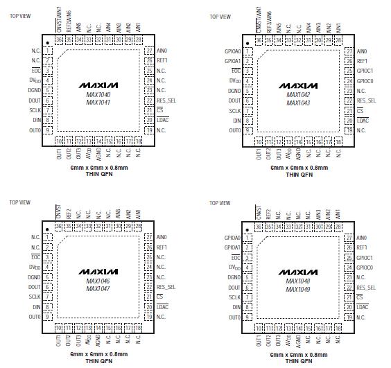
DescriptionThe MAX1040MAX1043/MAX1046MAX1049 integrate a multichannel, 10-bit, analog-to-digital converter (ADC) and a quad, 10-bit, digital-to-analog converter (DAC) in a single IC. The devices also include a temperature sensor and configurable general-purpose I/O ports (GPIOs) with a 25MHz SPI™-/QSPI™-/MICROWIRE™-compatible serial interface. The ADC is available in a 4 or an 8 inputchannel version. The four DAC outputs settle within 2.0s, and the ADC has a 300ksps conversion rate.
The MAX1040MAX1043/MAX1046MAX1049 include an internal reference (2.5V or 4.096V) providing a well-regulated, low-noise reference for both the ADC and DAC. Programmable reference modes for the ADC and DAC allow the use of an internal reference, an external reference, or a combination of both. Features such as an internal ±1°C accurate temperature sensor, FIFO, scan modes, programmable internal or external clock modes, data averaging, and AutoShutdown™ allow users to minimize both power consumption and processor requirements. The low glitch energy (4nV•s) and low digital feedthrough (0.5nV•s) of the integrated quad DACs make these devices ideal for digital control of fastresponse closed-loop systems.
The devices are guaranteed to operate with a supply voltage from +2.7V to +3.6V (MAX1041/MAX1043/MAX1047/ MAX1049) and from +4.75V to +5.25V (MAX1040/ MAX1042/MAX1046/MAX1048). These devices consume 2.5mA at 300ksps throughput, only 22A at 1ksps throughput, and under 0.2A in the shutdown mode. The MAX1042/MAX1043/MAX1048/MAX1049 offer four GPIOs that can be configured as inputs or outputs.
The MAX1040MAX1043/MAX1046MAX1049 are available in 36-pin thin QFN packages. All devices are specified over the -40°C to +85°C temperature range.

 MAX1040 Data Sheet


