Features: • M68HC11 CPU
• Power-saving stop and wait modes
• Low-voltage devices available (3.05.5 Vdc)
• 0, 256, 512, or 768 bytes of on-chip RAM, data retained during standby
• 0, 12, or 20 Kbytes of on-chip ROM or EPROM
• 0, 512, or 2048 bytes of on-chip EEPROM with block protect for security
• 2048 bytes of EEPROM with selectable base address in the MC68HC811E2
• Asynchronous non-return-to-zero (NRZ) serial communications interface (SCI)
• Additional baud rates available on MC68HC(7)11E20
• Synchronous serial peripheral interface (SPI)
• 8-channel, 8-bit analog-to-digital (A/D) converter
• 16-bit timer system:
Three input capture (IC) channels
Four output compare (OC) channels
One additional channel, selectable as fourth IC or fifth OC
• 8-bit pulse accumulator
• Real-time interrupt circuit
• Computer operating properly (COP) watchdog system
• 38 general-purpose input/output (I/O) pins:
16 bidirectional I/O pins
11 input-only pins
11 output-only pins
• Several packaging options:
52-pin plastic-leaded chip carrier (PLCC)
52-pin windowed ceramic leaded chip carrier (CLCC)
52-pin plastic thin quad flat pack, 10 mm x 10 mm (TQFP)
64-pin quad flat pack (QFP)
48-pin plastic dual in-line package (DIP), MC68HC811E2 only
56-pin plastic shrink dual in-line package, .070-inch lead spacing (SDIP)
Pinout Specifications
| Rating |
Symbol |
Value |
Unit |
| Supply voltage |
VDD |
0.3 to +7.0 |
V |
| Input voltage |
VIn |
0.3 to +7.0 |
V |
Current drain per pin(1) excluding VDD, VSS, AVDD,
VRH, VRL, andXIRQ/VPPE |
ID |
25 |
mA |
| Storage temperature |
TSTG |
55 to +150 |
°C |
DescriptionM68HC11E/D M68HC11E Family Technical Data
Pin Descriptions of M68HC11E
M68HC11 E-series MCUs are available packaged in:
• 52-pin plastic-leaded chip carrier (PLCC)
• 52-pin windowed ceramic leaded chip carrier (CLCC)
• 52-pin plastic thin quad flat pack, 10 mm x 10 mm (TQFP)
• 64-pin quad flat pack (QFP)
• 48-pin plastic dual in-line package (DIP), MC68HC811E2 only
• 56-pin plastic shrink dual in-line package, .070-inch lead spacing (SDIP)
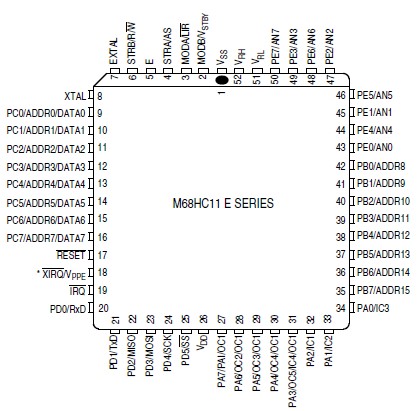
Most pins on these MCUs serve two or more functions, as described in the following paragraphs. Refer to Figure 1-2, Figure 1-3, Figure 1-4, Figure 1-5, and Figure 1-6 which show the M68HC11 E-series pin assignments for the PLCC/CLCC, QFP, TQFP, SDIP, and DIP packages.
Functional Description of M68HC11E
The central element in the SPI system is the block containing the shift register and the read data buffer. The system is single buffered in the transmit direction and double buffered in the receive direction. This means that new data for transmission cannot be written to the shifter until the previous transfer is complete; however, received data is transferred into a parallel read data buffer so the shifter is free to accept a second serial character. As long as the first character is read out of the read data buffer before the next serial character is ready to be transferred, no overrun condition occurs. A single MCU register address is used for reading data from the read data buffer and for writing data to the shifter.
The SPI status block represents the SPI status functions (transfer complete, write collision, and mode fault) performed by the serial peripheral status register (SPSR). The SPI control block represents those functions that control the SPI system through the serial peripheral control register (SPCR).

 M68HC11E Data Sheet


