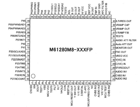
M61280M8-xxxFP

Features: • 3 line composite video signal inputs and 1 line S video signal input are available• Built-in 3 input audio switch with ATT output• Correspond to digital OSD• H output of emitter follower type (L at stopping, same as M61250BFP)• Selectable of ACL/ABCL•...

product image

M61280M8-xxxFP Picture
SeekIC No. : 004406419 Detail

M61280M8-xxxFP: Features: • 3 line composite video signal inputs and 1 line S video signal input are available• Built-in 3 input audio switch with ATT output• Correspond to digital OSD• H ou...

floor Price/Ceiling Price

Part Number:
M61280M8-xxxFP
Supply Ability:
5000

Price Break

  • Qty
  • 1~5000
  • Unit Price
  • Negotiable
  • Processing time
  • 15 Days
Total Cost: $ 0.00

SeekIC Buyer Protection PLUS - newly updated for 2013!

  • Escrow Protection.
  • Guaranteed refunds.
  • Secure payments.
  • Learn more >>

Month Sales

268 Transactions

Rating

evaluate  (4.8 stars)

Upload time: 2024/11/27

Payment Methods

All payment methods are secure and covered by SeekIC Buyer Protection PLUS.

Notice: When you place an order, your payment is made to SeekIC and not to your seller. SeekIC only pays the seller after confirming you have received your order. We will also never share your payment details with your seller.
Product Details

Description


Features:

• 3 line composite video signal inputs and 1 line S video signal input are available
• Built-in 3 input audio switch with ATT output
• Correspond to digital OSD
• H output of emitter follower type (L at stopping, same as M61250BFP)
• Selectable of ACL/ABCL
• Built-in H OSC resonator
• Built-in vertical saw tooth generator
• Correspond to fsc clock output
• Built-in 5V & 8V regulator
• Built-in MCU reset circuit
• Built-in 8bit MCU
• ROM: 32kByte, RAM: 1152byte


Application

• NTSC color television receivers


Pinout

  Connection Diagram


Specifications

Item Symbol Condition Ratings Unit
Power supply voltage (ASIC) Vcc (ASIC)   6.0, 10.0 V
Power supply voltage (MCU) Vcc (MCU) Measured with reference
to pin Vss. Output
transistor in shut-off
state.
0.3 to 6 V
Input voltage (MCU: CNVSS) VI (MCU) 0.3 to VCC+0.3 V
Input voltage (MCU: P00 to P07, P11 to
P14, P20 to 27, P40 to P45, RESET,
CVIN)
VI (MCU) 0.3 to VCC+0.3 V
Output voltage (MCU: P00 to P07, P11
to P14, P20 to 27, P40, P41)
VO (MCU)   0.3 to VCC+0.3 V
Circuit current (MCU: P11 to P14, P20
to P27, P40, P41)
IOH (MCU)   0 to 1 (Note 1) mA
Circuit current (MCU: P00 to P07, P20
to P23, P40, P41)
IOL1 (MCU)   0 to 2 (Note 2) mA
Circuit current (MCU: P11 to P14) IOL2 (MCU)   0 to 6 (Note 2) mA
Circuit current (MCU: P24 to P27) IOL3 (MCU)   0 to 10 (Note 2) mA
Power dissipation Pd Ta = 25°C 2000 mW
Thermal reduction Kt   20 mW/°C
Operating ambient temperature Topr   10 to 65 °C
Storage temperature Tstg   40 to 125 °C
Notes: 1. The sum of currents flowing from the IC should not exceed 20 mA.
2. The sum of currents flowing into the IC (IOL1+IOL2) should not exceed 30 mA.
3. Pin names for the different quantities are given as follows.
(1) Dedicated pins: Dedicated pin name
(2) Double/triple-function ports
*When standards are the same: I/O port name
*When standard of functions other than the I/O port are different: function pin name


Customers Who Bought This Item Also Bought

Margin,quality,low-cost products with low minimum orders. Secure your online payments with SeekIC Buyer Protection.
RF and RFID
Boxes, Enclosures, Racks
Soldering, Desoldering, Rework Products
Tapes, Adhesives
803
View more