M54HC113

Features: HIGH SPEED fMAX = 71 MHz (TYP.) at VCC = 5 VLOWPOWER DISSIPATION ICC = 2Aat AT TA = 25 °C HIGH NOISE IMMUNITY VNIH = VNIL = 28 % VCC (MIN.) OUTPUT DRIVE CAPABILITY 10 LSTTL LOADS SYMMETRICAL OUTPUT IMPEDANCE IOH = IOL = 4 mA (MIN.) BALANCEDPROPAGATION DELAYS tPLH = tPHL WIDE OPERATING VO...

product image

M54HC113 Picture
SeekIC No. : 004405809 Detail

M54HC113: Features: HIGH SPEED fMAX = 71 MHz (TYP.) at VCC = 5 VLOWPOWER DISSIPATION ICC = 2Aat AT TA = 25 °C HIGH NOISE IMMUNITY VNIH = VNIL = 28 % VCC (MIN.) OUTPUT DRIVE CAPABILITY 10 LSTTL LOADS SYMMETRIC...

floor Price/Ceiling Price

Part Number:
M54HC113
Supply Ability:
5000

Price Break

  • Qty
  • 1~5000
  • Unit Price
  • Negotiable
  • Processing time
  • 15 Days
Total Cost: $ 0.00

SeekIC Buyer Protection PLUS - newly updated for 2013!

  • Escrow Protection.
  • Guaranteed refunds.
  • Secure payments.
  • Learn more >>

Month Sales

268 Transactions

Rating

evaluate  (4.8 stars)

Upload time: 2024/11/27

Payment Methods

All payment methods are secure and covered by SeekIC Buyer Protection PLUS.

Notice: When you place an order, your payment is made to SeekIC and not to your seller. SeekIC only pays the seller after confirming you have received your order. We will also never share your payment details with your seller.
Product Details

Description


Features:

HIGH SPEED fMAX = 71 MHz (TYP.) at VCC = 5 V
LOWPOWER DISSIPATION ICC = 2A at  AT TA = 25 °C
HIGH NOISE IMMUNITY VNIH = VNIL = 28 % VCC (MIN.)
OUTPUT DRIVE CAPABILITY 10 LSTTL LOADS
SYMMETRICAL OUTPUT IMPEDANCE IOH = IOL = 4 mA (MIN.)
BALANCEDPROPAGATION DELAYS tPLH = tPHL
WIDE OPERATING VOLTAGE RANGE VCC (OPR) = 2 V TO 6 V
PIN AND FUNCTION COMPATIBLE WITH 54/74LS113


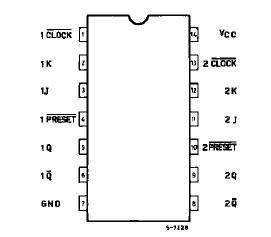
Pinout

  Connection Diagram


Specifications

Symbol
Parameter
Value
Unit
VCC
Supply Voltage
-0.5 to +7
V
VI
DC Input Voltage
-0.5 to VCC + 0.5
V
VO
DC Output Voltage
-0.5 to VCC + 0.5
V
IIK
DC Input Diode Current
± 20
mA
IOK
DC Output Diode Current
± 20
mA
IO
DC Output Source Sink Current Per Output Pin
± 25
mA
ICC or IGND
DC VCC or Ground Current
± 50
mA
PD
Power Dissipation
500 (*)
mW
Tstg
Storage Temperature
-65 to +150
°C
TL
Lead Temperature (10 sec)
300
°C
AbsoluteMaximumRatings are those values beyond whichdamage tothe device may occur. Functional operation under these condition isnotimplied.
(*) 500 mW: 65 derate to 300mWby 10mW/: 65 to85


Description

The M54/74HC113 is a high speed CMOSDUAL JK FLIP FLOP WITH PRESET fabricated in silicon gate C2MOS technology. It has the same high speed performance of LSTTL combined with true CMOSlowpower consumption. This circuit offers individual J, K, set, and clock inputs. These monolithic dual flip-flops are designed so that when the clock goes HIGH, the inputs are enabled and data will be accepted. The logic level of the J and K inputs may be allowed to change when the clock pulse is HIGH and the bistable will function as shown in the truth table as long as minimum set-up times are observed. Input data is transferred to the outputs on the negative-going edge of the clock pulse. All inputs of M54/74HC113  are equipped with protection circuits against static discharge and transient excess voltage.


Customers Who Bought This Item Also Bought

Margin,quality,low-cost products with low minimum orders. Secure your online payments with SeekIC Buyer Protection.
Computers, Office - Components, Accessories
Power Supplies - Board Mount
Motors, Solenoids, Driver Boards/Modules
Static Control, ESD, Clean Room Products
Circuit Protection
View more