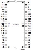
Features: ` Multiple Memories on a Single Chip: 4 Mbit Flash Memory (organised as 8 sectors) 256 Kbit EEPROM 64 Byte One Time Programmable Memory `CONCURRENT Mode (Read Flash while writing to EEPROM) ` WRITE, PROGRAM and ERASE Status Bits ` 2.7V to 3.6V Single Supply Voltage for PROGRAM, ERASE...
M39432: Features: ` Multiple Memories on a Single Chip: 4 Mbit Flash Memory (organised as 8 sectors) 256 Kbit EEPROM 64 Byte One Time Programmable Memory `CONCURRENT Mode (Read Flash while writing to EE...
SeekIC Buyer Protection PLUS - newly updated for 2013!
268 Transactions
All payment methods are secure and covered by SeekIC Buyer Protection PLUS.
Symbol | Parameter |
Value |
Unit |
TA | Ambient Operating Temperature |
40 to 85 |
|
TBIAS 1 | Temperature Under Bias |
50 to 125 |
|
TSTG 1 | Storage temperature |
65 to 150 |
|
VIO 1,2 | Input or Output Voltages(except A9) |
0.6 to 7 |
V |
VCC 1 | Supply Voltage |
0.6 to 7 |
V |
VA9, VG, VEF 1,2 | A9, G, EF Voltage |
0.6 to 13.5 |
V |
Note: 1. Stresses above those listed may cause permanent damage to the device. These are stress ratings only and operation of the device at these or any other conditions above those indicated in the Operating sections of this specification is not implied. Exposure to Absolute Maximum Rating conditions for extended periods may affect device reliability. Please see the STMicroelectronics SURE Program and other relevant quality documents.
2. Minimum voltage may undershoot to 2 V, during transition and for less than 20 ns.
The M39432 is a single supply voltage memory device combining Flash memory and EEPROM on a single chip. The memory is mapped in two.
The M39432 EEPROM block may be written bytewise or by a page at a time (up to 64 bytes). The integrity of the data can be secured with the help of the Software Data Protection (SDP).
The M39432 Flash Memory block offers 8 sectors, each one 64 KByte in size. Each sector may be erased individually, and programmed a byte at a time. Each sector can be separately protected and unprotected against Program and Erase. Sector erasure may be suspended, while data is read from other sectors of the Flash memory block (or from the EEPROM block), and then resumed. The Flash memory block is functionally compatible with the M29W040 (4 Mbit Single Voltage Flash Memory).
During a Program or Erase cycle in the Flash memory or during a Write cycle in the EEPROM, the status of the M39432 internal logic can be read on the Data Output pins DQ7, DQ6, DQ5 and DQ3.