M38D59FFFP

Features: • Basic machine-language instructions ................................. 71• The minimum instruction execution time ................... 0.32 s (at 12.5 MHz oscillation frequency)• Memory size (QzROM version) ROM ........................................................ 32...

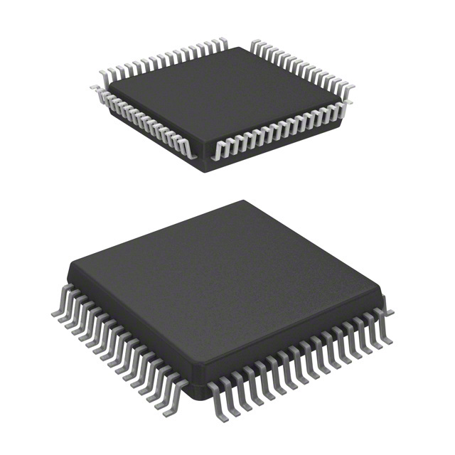
product image

M38D59FFFP Picture
SeekIC No. : 004405126 Detail

M38D59FFFP: Features: • Basic machine-language instructions ................................. 71• The minimum instruction execution time ................... 0.32 s (at 12.5 MHz oscillation frequency...

floor Price/Ceiling Price

Part Number:
M38D59FFFP
Supply Ability:
5000

Price Break

  • Qty
  • 1~5000
  • Unit Price
  • Negotiable
  • Processing time
  • 15 Days
Total Cost: $ 0.00

SeekIC Buyer Protection PLUS - newly updated for 2013!

  • Escrow Protection.
  • Guaranteed refunds.
  • Secure payments.
  • Learn more >>

Month Sales

268 Transactions

Rating

evaluate  (4.8 stars)

Upload time: 2024/11/27

Payment Methods

All payment methods are secure and covered by SeekIC Buyer Protection PLUS.

Notice: When you place an order, your payment is made to SeekIC and not to your seller. SeekIC only pays the seller after confirming you have received your order. We will also never share your payment details with your seller.
Product Details

Description


Features:

• Basic machine-language instructions ................................. 71
• The minimum instruction execution time ................... 0.32 s
   (at 12.5 MHz oscillation frequency)
• Memory size (QzROM version)
   ROM ........................................................ 32 K to 60 K bytes
   RAM ......................................................... 1536 to 2048 bytes
• Memory size (Flash memory version)
   ROM ...................................................................... 60 K bytes
   RAM ...................................................................... 2048 bytes
• Programmable input/output ports .. 59 (common to SEG: 36)
• Interrupts ............................................. 17 sources, 16 vectors
   (Key input interrupt included)
• Timers ..................................................... 8-bit * 4, 16-bit * 2
• Serial interface
   Serial I/O1...............8-bit * 1 (UART or Clock-synchronized)
   Serial I/O2 .............................. 8-bit * 1 (Clock-synchronized)
• PWM .......... 10-bit * 2, 16-bit * 1 (common to IGBT output)
• A/D converter .......................................... 10-bit * 8 channels
   (A/D converter can be operated in low-speed mode.)
• Watchdog timer ......................................................... 8-bit * 1
• ROM correction function ....................... 32 bytes * 2 vectors
• LED direct drive port ............................................................ 6
   (average current: 15 mA, peak current: 30 mA, total current: 90 mA)
• LCD drive control circuit
   Bias ............................................................................ 1/2, 1/3
   Duty ............................................................... Static, 2, 3, 4, 8
   Common output ................................................................. 4/8
   Segment output .............................................................. 32/36
• Main clock generating circuit ............................................... 1
   (connect to external ceramic resonator or on-chip oscillator)
• Sub-clock generating circuit ..................................................1
   (connect to external quartz-crystal oscillator)
• Power source voltage (QzROM version)
   [In frequency/2 mode]
   f(XIN) 12.5 MHz.............................................. 4.5 to 5.5 V
   f(XIN) 8 MHz................................................... 4.0 to 5.5 V
   f(XIN) 4 MHz................................................... 2.0 to 5.5 V
   f(XIN) 2 MHz................................................... 1.8 to 5.5 V
   [In frequency/4 mode]
   f(XIN) 16 MHz................................................. 4.5 to 5.5 V
   f(XIN) 8 MHz................................................... 2.0 to 5.5 V
   f(XIN) 4 MHz................................................... 1.8 to 5.5 V
   [In frequency/8 mode]
   f(XIN) 16 MHz................................................. 4.5 to 5.5 V
   f(XIN) 8 MHz................................................... 2.0 to 5.5 V
   f(XIN) 4 MHz................................................... 1.8 to 5.5 V
   [In low-speed mode].............................................. 1.8 to 5.5 V
   Note. 12.5 MHz < f(XIN) 16 MHz is not available in the frequency/2 mode.
• Power source voltage (Flash memory version)
   [In frequency/2 mode]
   f(XIN) 12.5 MHz.............................................. 4.5 to 5.5 V
   f(XIN) 8 MHz................................................... 4.0 to 5.5 V
   f(XIN) 4 MHz................................................... 2.7 to 5.5 V
   [In frequency/4 mode]
   f(XIN) 16 MHz................................................. 4.5 to 5.5 V
   f(XIN) 8 MHz................................................... 2.7 to 5.5 V
   [In frequency/8 mode]
   f(XIN) 16 MHz................................................. 4.5 to 5.5 V
   f(XIN) 8 MHz................................................... 2.7 to 5.5 V
   [In low-speed mode].............................................. 2.7 to 5.5 V
   Note. 12.5 MHz < f(XIN) 16 MHz is not available in the frequency/2 mode.
• Power dissipation (QzROM version)
• In frequency/2 mode ..................................... Typ. 32 mW
   (VCC = 5 V, f(XIN) = 12.5 MHz, Ta = 25°C)
• In low-speed mode ........................................ Typ. 18 W
   (VCC = 2.5 V, f(XIN) = stop, f(XCIN) = 32 kHz, Ta = 25°C)
• Power dissipation (Flash memory version)
• In frequency/2 mode ..................................... Typ. 20 mW
   (VCC = 5 V, f(XIN) = 12.5 MHz, Ta = 25°C)
• In low-speed mode ...................................... Typ. 1.1 mW
   (VCC = 2.7 V, f(XIN) = stop, f(XCIN) = 32 kHz, Ta = 25°C)
• Operating temperature range ............................... −20 to 85°C


Application

  ·Household products, Consumer electronics, etc.


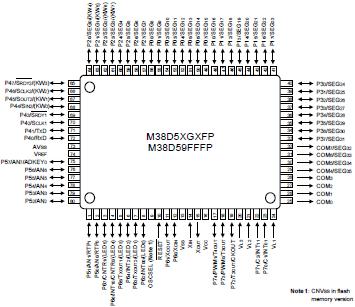
Pinout

  Connection Diagram


Specifications

Symbol Parameter Conditions
Ratings
Unit
VCC Power source voltage All voltages are based on VSS.
When an input voltage is measured,
output transistors are cut off.
0.3 to 6.5
V
VI Input voltage
P00−P07, P10−P17, P20−P27, P30−P37
P40−P47, P50−P57, P60−P67, P70−P74
0.3 to VCC +0.3
V
VI Input voltage VL1
0.3 to VL2
V
VI Input voltage VL2
VL1 to VL3
V
VI Input voltage VL3
VL2 to 6.5
V
VI Input voltage C1, C2
−0.3 to 6.5
V
VI Input voltage RESET, XIN
−0.3 to VCC+0.3
V
VI Input voltage OSCSEL
−0.3 to 8.0
V
VO Output voltage C1, C2
−0.3 to 6.5
V
VO Output voltage P00−P07, P10−P17, P20−P27, P30−P37 At output port
0.3 to VCC +0.3
V
At segment output
0.3 to VL3+3.0
V
VO Output voltage P40−P47, P50−P57, P60−P67, P72−P74  
0.3 to VCC+0.3
V
VO Output voltage VL3
0.3 to 6.5
V
VO Output voltage VL2, SEG32−SEG35, COM0−COM3
0.3 to VL3+0.3
V
VO Output voltage XOUT
0.3 to VCC+0.3
V
Pd Power dissipation Ta = 25
300
mW
Topr Operating temperature  
20 to 85
Tstg Storage temperature  
40 to 150


Description

The 38D5 Group is the 8-bit microcomputer based on the 740 Family core technology.

The 38D5 Group is pin-compatible with the 38C5 Group. The 38D5 Group has an LCD drive control circuit, an A/D converter, a serial interface, and a ROM correction function as additional functions.

The QzROM version and the flash memory version 38D5 Group are available. The flash memory version does not have a selection function for the oscillation start mode. Only the on-chip oscillator starts oscillating.

The 38D5 Group include variations of memory size, and packaging. For details, refer to the section on part numbering.


Customers Who Bought This Item Also Bought

Margin,quality,low-cost products with low minimum orders. Secure your online payments with SeekIC Buyer Protection.
Static Control, ESD, Clean Room Products
Isolators
Computers, Office - Components, Accessories
View more