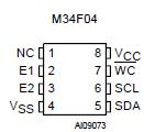
Features: · Two Wire I2C Serial Interface Supports 400 kHz Protocol· 2.5 to 5.5V Single Supply Voltage:· Hardware Write Control of the top half of memory (addresses 100h to 1FFh)· BYTE and PAGE WRITE (up to 16 Bytes)· RANDOM and SEQUENTIAL READ Modes· Self-Timed Programming Cycle· Automatic Addres...
M34F04: Features: · Two Wire I2C Serial Interface Supports 400 kHz Protocol· 2.5 to 5.5V Single Supply Voltage:· Hardware Write Control of the top half of memory (addresses 100h to 1FFh)· BYTE and PAGE WRIT...
SeekIC Buyer Protection PLUS - newly updated for 2013!
268 Transactions
All payment methods are secure and covered by SeekIC Buyer Protection PLUS.
Symbol |
Parameter |
Min. |
Max. |
Unit |
TSTG | Storage Temperature |
-65 |
150 |
|
TLEAD | Lead Temperature during Soldering 1 |
260 2 |
||
VIO | Input or Output range |
-0.6 |
6.5 |
V |
VCC | Supply Voltage |
-0.3 |
6.5 |
V |
VESD | Electrostatic Discharge Voltage (Human Body model) 3 |
-4000 |
4000 |
V |
The M34F04 is an electrically erasable programmable memory (EEPROM), organized as 512 x 8.
M34F04 is compatible with the I2C memory protocol. This is a two wire serial interface that uses a bi-directional data bus and serial clock. The devices carry a built-in 4-bit Device Type Identifier code (1010) in accordance with the I2C bus definition.
The M34F04 behaves as a slave in the I2C protocol, with all memory operations synchronized by the serial clock. Read and Write operations M34F04 are initiated by a Start condition, generated by the bus master. The Start condition is followed by a Device Select Code and RW bit (as described in Table 2), terminated by an acknowledge bit.
When writing data to the memory, the M34F04 inserts an acknowledge bit during the 9th bit time, following the bus master's 8-bit transmission. When data is read by the bus master, the bus master acknowledges the receipt of the data byte in the same way. Data transfers of M34F04 are terminated by a Stop condition after an Ack for Write, and after a NoAck for Read.