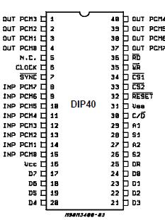
Features: ·256 INPUT AND 256 OUTPUT CHANNEL CMOS DIGITAL SWITCHING MATRIX COM-
·PATIBLEWITH M088 BUILDING BLOCK DESIGNED FOR LARGE CAPACITY ELECTRONICEXCHANGES, SUB.
SYSTEMS AND PABX NO EXTRA PIN NEEDED FOR NOT-BLOCKING SINGLE STAGE AND HIGHER CAPACITY
·SYNTHESIS BLOCKS (512 or 1024 channels) EUROPEAN TELEPHONE STANDARD COM.
PATIBLE (32 serial channels per frame) PCM INPUTS AND OUTPUTS MUTUALLY
·COMPATIBLE ACTUAL INPUT-OUTPUT CHANNEL CONNECTIONS
STORED AND MODIFIED VIA AN ON CHIP 8-BIT PARALLEL MICROPROCES.
SOR INTERFACE .TYPICAL BIT RATE : 2Mbit/s TYPICAL SYNCHRONIZATION RATE : 8KHz
(time frame is 125ms)
·5V P0WER SUPPLY
·CMOS & TTL INPUT/OUTPUT LEVELS COM. PATIBLE
·HIGH DENSITY ADVANCED 1.2mm HCMOS3 PROCESS Application256PCM links network (160 or 192 DSM) : the 32 x 32 link module shown on the next page.
2048PCM links network (1792 or 2048 DSM) : the 256 x 256 link network is shown above.Pinout Specifications
|
Symbol |
Parameter |
Test Conditions |
Unit |
| VCC |
Supply Voltage |
-0.3 to 7 |
V |
| VI |
Input Voltage |
-0.3 to VCC+0.3 |
V |
| VO |
Off State Output Voltage |
-0.3 to VCC+0.3 |
V |
| IO |
Current at Digital Outputs |
30 |
mA |
| Ptot |
Total Package Power Dissipation |
1.5 |
W |
| Tstg |
Storage Temperature Range |
-65 to 150 |
|
| Top |
Operating Temperature Range |
0 to 70 |
|
Stresses above those l isted under " Absolute Maximum Ratings" may cause permanent damage to the device. This is a stress ratings only and functional operation of the device at these or any other conditions above those indicated in the operating condi tions of this specification is not implied. Exposure to absolute maximum rating condi tions for extended periods may affect device rel iabili ty.
DescriptionThe M3488 is intendedfor largetelephoneswitching systems,mainly central exchanges,digital line concentrators and private branch exchanges where a distributed microcomputer control approach is extensively used. M3488 consists of a speech memory (SM), a controlmemory (CM), a serial/parallel and a parallel/serial converter, an internal parallel bus, an interface (8 data lines, 11 control signals) and dedicated control logic.
By means of repeated clock division two timebases are generated. M3488 is preset from an external synchronization signal to two specific count numbers so that sequential scanning of the bases give synchronous addresses to the memories and I/O channel controls. Different preset count numbers of M3488 are needed because of processing delays and datapath direction.Thetimebasefor theinputchannels is delayed and the timebase for output channels is advancedwith respect to the actual time.
Each serial PCM input channel M3488 is converted to parallel data and stored in the speech memory at the beginning of any new time slot (according to first timebase) in the location determined by input pin number and time slot number. The controlmemory CM maintains the correspondencesbetween input and output channels. More exactly, for any output pin/outputchannelcombination the controlmemory gives either the full address of the speech memory location involved in the PCM M3488 transfer or an 8-bit word to be supplied to theparallel/serial output converter. A9th bit at each CMlocation defines the data source for output links, low for SM, high for CM.
The late timebase is used to scan the output channels and to determine the pins of M3488 to be serviced within each channel ; enough idle cycles are left to the microprocessor for asynchronousinstruction processing.
Two 8-bit registers OR1 and OR2 supply feedback datafor control or diagnosticpurposes;OR1 comes from internal bus i.e. frommemories, OR2 gives an opcode copy and additional data of M3488 to the microcomputer. A four byte-five bit stack register and an instruction register, under microcomputer control, store input data available at the interface.
Dedicatedlogic, undercontrolof themicroprocessorinterface, extracts the 0 channel content of any selected PCM input bus, using spare cycles of SM.

 M3488 Data Sheet


