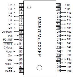
Features: ·Minimum instruction execution time When f(XIN) is selected for system clock ....................... 1.5ms (f(XIN)=2.0 MHz, VDD=4.5 V to 5.5 V) When f(XIN)/4 is selected for system lock .................... 2.86ms (f(XIN)=4.2 MHz,VDD=2.0 V to 5.5 V)·Supply voltage...........................
M34570M8-XXXFP: Features: ·Minimum instruction execution time When f(XIN) is selected for system clock ....................... 1.5ms (f(XIN)=2.0 MHz, VDD=4.5 V to 5.5 V) When f(XIN)/4 is selected for system lock .....
SeekIC Buyer Protection PLUS - newly updated for 2013!
268 Transactions
All payment methods are secure and covered by SeekIC Buyer Protection PLUS.
Features: `Minimum instruction execution time ................................ ..0.68 s(at 4.4 MHz...
·Minimum instruction execution time
When f(XIN) is selected for system clock ....................... 1.5ms
(f(XIN)=2.0 MHz, VDD=4.5 V to 5.5 V)
When f(XIN)/4 is selected for system lock .................... 2.86ms
(f(XIN)=4.2 MHz,VDD=2.0 V to 5.5 V)
·Supply voltage
............................ 2.5 V to 5.5 V (One Time PROM version)
. .................................... 2.0 V to 5.5 V (Mask ROM version
· System clock switch function.................. f(XIN)/4 or not divided
· Timers
Timer 1... 10-bit timer with a reload register and carrier wave output auto-control function
Timer 2 ................................ 8-bit timer with a reload register
Timer 3... 8-bit timer with two reload registers and carrier wave generation function
· Interrupt ....................................................................4 sources
· Power-on reset circuit
· Watchdog timer ............................................................ .16 bits
· Key-on wakeup function (Ports P0, P1, and P4, ON/OFF of port P4 can be switched)
· Pull-up transistor (Ports P0, P1, and P4, ON/OFF of port P4 can be switched)
· Voltage drop detection circuit
· Clock generating circuit (ceramic resonance)
Symbol |
Parameter |
Conditions |
Ratings |
Unit |
VDD | Supply voltage |
0.3 to 7.0 |
V | |
VI | Input voltage P0, P1, P2, P3, P4, RESET, XIN, VDCE |
0.3 to VDD+0.3 |
V | |
VO | Output voltage P0, P1, P3, D | Output transistors in cut-off state |
0.3 to VDD+0.3 |
V |
VO | Output voltage CARR, XOUT |
0.3 to VDD+0.3 |
V | |
Pd | Power dissipation |
300 |
mW | |
Topr | Operating temperature range |
-20 to 70 |
||
Tstg | Storage temperature range |
40 to 125 |
The 4570 Group is a 4-bit single-chip microcomputer designed with CMOS technology. Its CPU is that of the 4500 series using a simple, high-speed instruction set. The computer of 4570 is equipped with a carrier wave output circuit for remote control, an 8-bit timer with a reload register, a 10-bit timer with a reload register, and an 8-bit timer with two reload registers.
The various microcomputers in the 4570 Group include variations of the built-in memory size. The mask ROM version and One Time PROM version of 4570 Group are produced as shown in the table below.