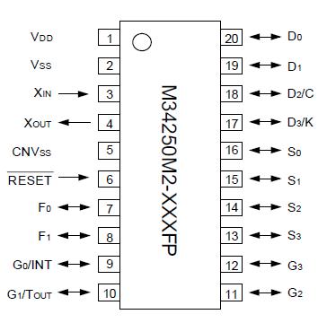
M34250M2-XXXFP

Features: • Minimum instruction execution time ............................. 1.0 ms(at 4.0 MHz system clock frequency, VDD=4.5 V to 5.5 V)• Supply voltage4.5 V to 5.5 V (at 4.0 MHz system clock frequency)2.5 V to 5.5 V (at 1.0 MHz system clock frequency)2.2 V to 5.5 V (at 1.0 MHz syste...

product image

M34250M2-XXXFP Picture
SeekIC No. : 004404731 Detail

M34250M2-XXXFP: Features: • Minimum instruction execution time ............................. 1.0 ms(at 4.0 MHz system clock frequency, VDD=4.5 V to 5.5 V)• Supply voltage4.5 V to 5.5 V (at 4.0 MHz syste...

floor Price/Ceiling Price

Part Number:
M34250M2-XXXFP
Supply Ability:
5000

Price Break

  • Qty
  • 1~5000
  • Unit Price
  • Negotiable
  • Processing time
  • 15 Days
Total Cost: $ 0.00

SeekIC Buyer Protection PLUS - newly updated for 2013!

  • Escrow Protection.
  • Guaranteed refunds.
  • Secure payments.
  • Learn more >>

Month Sales

268 Transactions

Rating

evaluate  (4.8 stars)

Upload time: 2024/11/27

Payment Methods

All payment methods are secure and covered by SeekIC Buyer Protection PLUS.

Notice: When you place an order, your payment is made to SeekIC and not to your seller. SeekIC only pays the seller after confirming you have received your order. We will also never share your payment details with your seller.
Product Details

Description


Features:

• Minimum instruction execution time ............................. 1.0 ms
(at 4.0 MHz system clock frequency, VDD=4.5 V to 5.5 V)
• Supply voltage
4.5 V to 5.5 V (at 4.0 MHz system clock frequency)
2.5 V to 5.5 V (at 1.0 MHz system clock frequency)
2.2 V to 5.5 V (at 1.0 MHz system clock frequency: only for Mask ROM version)
• Timer
Timer 1 ................................ 8-bit timer with a reload register
• Interrupt ................................................................... 2 sources
• CR oscillation circuit (Capacitor and Resistor connected externally)
• Logic operation instruction
• RAM back-up function
• Key-on wakeup function (ports G and S, INT pin)


Application

Electric household appliances, consumer electronics products (mouse, etc.)


Pinout

  Connection Diagram


Specifications

Symbol Parameter Conditions
Value
Unit
VDD (*) Supply Voltage  
0.3 to 7.0
V
Vi Input Voltage XIN, G0G3, D2/C, D3/K  
0.3 to VDD+0.3
V
Vi Input voltage F0, F1, S0S3, D0, D1, RESET   0.3 to 8.0 V
VO Output voltage XOUT   0.3 to VDD+0.3 V
VO Output voltage F0, F1, S0S3, D0, D1   0.3 to 8.0 V
VO Output voltage G0G3, D2/C, D3/K  
0.3 to VDD+0.3
V
pd Power dissipation Output transistors
in cut-off state
300
mW
Ptot Operating temperature range Ta = 25
20 to 850
Tstg Storage temperature range  
-40 to 125


Description

The 4250 Group is a 4-bit single-chip microcomputer designed with CMOS technology. Its CPU is that of the 720 series using a simple instruction set. The computer is equipped with one 8-bit timer which has a reload register and the interrupt function.

The various microcomputers in the 4250 Group include variations of the built-in memory type as shown in the table below.


Customers Who Bought This Item Also Bought

Margin,quality,low-cost products with low minimum orders. Secure your online payments with SeekIC Buyer Protection.
Crystals and Oscillators
Test Equipment
Static Control, ESD, Clean Room Products
Batteries, Chargers, Holders
Transformers
View more