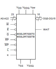
Features: SUPPLY VOLTAGE
VDD = 1.7V to 2.0V for program, erase an read
VDDQ = 1.7V to 2.0V for I/O Buffers
VPP = 9V for fast program (12V tolerant)
SYNCHRONOUS / ASYNCHRONOUS READ
Synchronous Burst Read mode: 54MHz
Asynchronous Page Read mode
Random Access: 85ns
SYNCHRONOUS BURST READ SUSPEND
PROGRAMMING TIME
10s typical Word program time using Buffer Program
MEMORY ORGANIZATION
Multiple Bank Memory Array: 8 Mbit Banks
Parameter Blocks (Top or Bottom location)
DUAL OPERATIONS
program/erase in one Bank while read in others
No delay between read and write operations
BLOCK LOCKING
All blocks locked at power-up
Any combination of blocks can be locked with zero latency
WP for Block Lock-Down
Absolute Write Protection with VPP = VSS
SECURITY
64 bit unique device number
2112 bit user programmable OTP Cells
COMMON FLASH INTERFACE (CFI)
100,000 PROGRAM/ERASE CYCLES per BLOCK
ELECTRONIC SIGNATURE
Manufacturer Code: 20h
Top Device Code: 88C4h.
Bottom Device Code: 88C5h
PACKAGE
Compliant with Lead-Free Soldering Processes
Lead-Free VersionsPinout Specifications
|
Symbol |
Parameter |
Value |
Unit |
|
Min |
Max |
|
TA |
Ambient Operating Temperature |
25 |
85 |
°C |
|
TBIAS |
Temperature Under Bias |
25 |
85 |
°C |
|
TSTG |
Storage Temperature |
65 |
125 |
°C |
|
TLEAD |
Lead Temperature during Soldering |
|
(1) |
°C |
|
VIO |
Input or Output Voltage |
0.5 |
3.8 |
V |
|
VDD |
Supply Voltage |
0.2 |
2.5 |
V |
|
VDDQ |
Input/Output Supply Voltage |
0.2 |
2.5 |
V |
|
VPP |
Program Voltage |
0.2 |
14 |
V |
|
IO |
Output Short Circuit Current |
|
100 |
mA |
|
tVPPH |
Time for VPP at VPPH |
|
100 |
hours |
DescriptionThe M30L0R7000T0/B0 is a 128 Mbit (8Mbit x16) non-volatile Flash memory that may be erased electrically at block level and programmed in-system on a Word-by-Word basis using a 1.7V to 2.0V VDD supply for the circuitry and a 1.7V to 2.0V VDDQ supply for the Input/Output pins. An optional 9V VPP power supply is provided to speed up factory programming.
The device features an asymmetrical block architecture and is based on a multi-level cell technology. M30L0R7000T0/B0 has an array of 131 blocks, and is divided into 8 Mbit banks. There are 15 banks each containing 8 main blocks of 64 KWords, and one parameter bank containing 4 parameter blocks of 16 KWords and 7 main blocks of 64 KWords. The Multiple Bank Architecture allows Dual Operations, while programming or erasing in one bank, read operations are possible in other banks. Only one bank at a time is allowed to be in program or erase mode. It is possible to perform burst reads that cross bank boundaries. The bank architecture is summarized in Table 2., and the memory maps are shown in Figure 4. The Parameter Blocks are located at the top of the memory address space for the M30L0R7000T0, and at the bottom for the M30L0R7000B0.
Each block M30L0R7000T0 can be erased separately. Erase can be suspended, in order to perform program in any other block, and then resumed. Program can be suspended to read data in any other block and then resumed. Each block can be programmed and erased over 100,000 cycles using the supply voltage VDD. There is a Buffer Enhanced Factory programming command available to speed up programming.
Program and erase commands M30L0R7000T0 are written to the Command Interface of the memory. An internal Program/Erase Controller takes care of the timings necessary for program and erase operations. The end of a program or erase operation can be detected and any error conditions identified in the Status Register. The command set required to control the memory is consistent with JEDEC standards.
The M30L0R7000T0 supports Synchronous Burst Read and Asynchronous Read from all blocks of the memory array; at power-up the device is configured for Asynchronous Read. In Synchronous Burst Read mode, data is output on each clock cycle at frequencies of up to 54MHz. The Synchronous Burst Read operation can be suspended and resumed.
The M30L0R7000T0 features an Automatic Standby mode. When the bus is inactive during Asynchronous Read operations, the device automatically switches to the Automatic Standby mode. In this condition the power consumption is reduced to the standby value and the outputs are still driven.
The M30L0R7000T0 features an instant, individual block locking scheme that allows any block to be locked or unlocked with no latency, enabling instant code and data protection. All blocks have three levels of protection. They can be locked and locked-down individually preventing any accidental programming or erasure. There is an additional hardware protection against program and erase. When VPP VPPLK all blocks are protected against program or erase. All blocks are locked at powerup.
The M30L0R7000T0 includes 17 Protection Registers and 2 Protection Register locks, one for the first Protection Register and the other for the 16 One-Time- Programmable (OTP) Protection Registers of 128 bits each. The first Protection Register is divided into two segments: a 64 bit segment containing a unique device number written by ST, and a 64 bit segment One-Time-Programmable (OTP) by the user. The user programmable segment can be permanently protected. Figure 5., shows the Protection Register Memory Map.
The memory M30L0R7000T0 is available in a TFBGA88, 8 x 10mm, 0.8mm pitch package.
In addition to the standard version, the packages are also available in Lead-free version, in compliance with JEDEC Std J-STD-020B, the ST ECOPACK 7191395 Specification, and the RoHS (Restriction of Hazardous Substances) directive.
All packages are compliant with Lead-free soldering processes.
The memory M30L0R7000T0 is supplied with all the bits erased (set to '1').

 M30L0R7000T0 Data Sheet


