M306V5ME-XXXSP

Features: • Memory size ..................................... ...<ROM>192K bytes <RAM> 5K bytes <OSD ROM> 61K bytes <OSD RAM> 2.2K bytes• Shortest instruction execution time ..... 100 ns (f(XIN)=10 MHz)• Power sourse voltage .......................... 4...

product image

M306V5ME-XXXSP Picture
SeekIC No. : 004404665 Detail

M306V5ME-XXXSP: Features: • Memory size ..................................... ...<ROM>192K bytes <RAM> 5K bytes <OSD ROM> 61K bytes <OSD RAM> 2.2K bytes• Shortest instruction ...

floor Price/Ceiling Price

Part Number:
M306V5ME-XXXSP
Supply Ability:
5000

Price Break

  • Qty
  • 1~5000
  • Unit Price
  • Negotiable
  • Processing time
  • 15 Days
Total Cost: $ 0.00

SeekIC Buyer Protection PLUS - newly updated for 2013!

  • Escrow Protection.
  • Guaranteed refunds.
  • Secure payments.
  • Learn more >>

Month Sales

268 Transactions

Rating

evaluate  (4.8 stars)

Upload time: 2024/11/27

Payment Methods

All payment methods are secure and covered by SeekIC Buyer Protection PLUS.

Notice: When you place an order, your payment is made to SeekIC and not to your seller. SeekIC only pays the seller after confirming you have received your order. We will also never share your payment details with your seller.
Product Details

Description


Features:

• Memory size ..................................... ...<ROM>192K bytes
                                                                <RAM> 5K bytes
                                                                <OSD ROM> 61K bytes
                                                                <OSD RAM> 2.2K bytes
• Shortest instruction execution time ..... 100 ns (f(XIN)=10 MHz)
• Power sourse voltage .......................... 4.5 V to 5.5V
• Power consumption ..............................250 mW
• Interrupts ............................................ 21 internal and 3 external interrupt sources, 4 software
                                                                 interrupt sources; 7 levels
• Multifunction 16-bit timer ...................... 2 output timers + 1 input timer + 5 timers
• Serial I/O .............................................. 4 units
                                                                 UART/clock synchronous: 2
                                                                 Multi-master I2C-BUS interface 0 (2 systems): 1
                                                                 Multi-master I2C-BUS interface 1 (1 systems): 1
• DMAC .................................................. 2 channels (trigger: 23 sources)
• A-D converter ...................................... 8 bits 5 6 channels
• D-A converter ...................................... 8 bits 5 2 channels
• Data slicer ........................................... 1 circuit
• HSYNC counter .................................... 1 circuit (2 systems)
• OSD function ....................................... 1 circuit
• Watchdog timer................................... 1 circuit
• Programmable I/O ............................... 46 lines
• Clock generating circuit ....................... 2 built-in clock generation circuits


Application

DESCRIPTION
OPERATION OF FUNCTIONAL BLOCKS
USAGE PRECAUTION
ITEM TO BE SUBMITTED WHEN ORDERING
ELECTRICAL CHARACTERISTICS
MASK ROM CONFIRMATION FORM
MARK SPECIFICATION FORM
ONE TIME PROM VERSION
PACKAGE OUTLINE


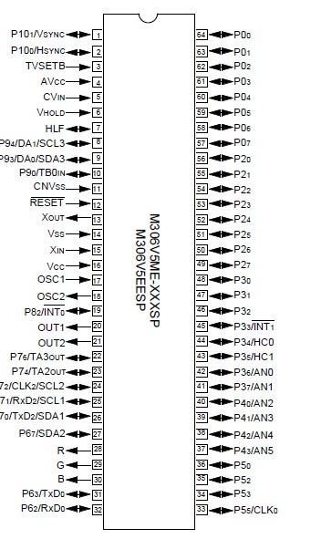
Pinout

  Connection Diagram


Specifications

Item Specification
No. of channels 2 (cycle steal method)
Transfer memory space • From any address in the 1M bytes space to a fixed address
• From a fixed address to any address in the 1M bytes space
• From a fixed address to a fixed address
(Note that DMA-related registers [002016 to 003F16] cannot be accessed)
Maximum No. of bytes transferred 128K bytes (with 16-bit transfers) or 64K bytes (with 8-bit transfers)
DMA request factors (Note) Falling edge or both edge of pin INT0
Falling edge of pin INT1
Timer A0 to timer A4 interrupt requests
Timer B0 to timer B2 interrupt requests
UART0 transmission and reception interrupt requests
UART2 transmission and reception interrupt requests
Multi-master I2C-BUS interface 0 interrupt request
Multi-master I2C-BUS interface 1 interrupt request
A-D conversion interrupt request
OSD1 and OSD2 interrupt requests
Data slicer interrupt request
VSYNC interrupt request
Software triggers
Channel priority DMA0 takes precedence if DMA0 and DMA1 requests are generated simultaneously
Transfer unit 8 bits or 16 bits
Transfer address direction forward/fixed (forward direction cannot be specified for both source and destination simultaneously)
Transfer mode • Single transfer mode
After the transfer counter underflows, the DMA enable bit turns to "0", and theDMAC turns inactive
• Repeat transfer mode
After the transfer counter underflows, the value of the transfer counter reload register is reloaded to the transfer counter.
The DMAC remains active unless a "0" is written to the DMA enable bit.
DMA interrupt request generation timing When an underflow occurs in the transfer counter
Active When the DMA enable bit is set to "1", the DMAC is active.
When the DMAC is active, data transfer starts every time a DMA transfer request signal occurs.
Inactive • When the DMA enable bit is set to "0", the DMAC is inactive.
• After the transfer counter underflows in single transfer mode
Forward address pointer andreload timing for transfer counter At the time of starting data transfer immediately after turning the DMAC active,the value of one of source pointer and destination pointer - the one specified for the forward direction - is reloaded to the forward direction address pointer, andthe value of the transfer counter reload register is reloaded to the transfer counter.
Writing to register Registers specified for forward direction transfer are always write enabled.
Registers specified for fixed address transfer are write-enabled when the DMA enable bit is "0".
Reading the register Can be read at any time.
However, when the DMA enable bit is "1", reading the register set up as the forward register is the same as reading the value of the forwardaddress pointer.


Description

The M306V5ME-XXXSP and M306V5EESP are single-chip microcomputers using the high-performance silicon gate CMOS process using a M16C/60 Series CPU core and are packaged in a 64-pin plastic molded SDIP. These single-chip microcomputers operate using sophisticated instructions featuring a high level of instruction efficiency. With 1M bytes of address space, they are capable of executing instructions at high speed. They also feature a built-in OSD display function and data slicer, making them ideal for controlling TV with a closed caption decoder.

The features of the M306V5EESP are similar to those of the M306V5ME-XXXSP except that this chip has a built-in PROM which can be written electrically.


Customers Who Bought This Item Also Bought

Margin,quality,low-cost products with low minimum orders. Secure your online payments with SeekIC Buyer Protection.
Discrete Semiconductor Products
Line Protection, Backups
Inductors, Coils, Chokes
Static Control, ESD, Clean Room Products
Integrated Circuits (ICs)
RF and RFID
View more