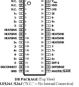
Features: Auto-Selectable LVD or Single- Ended Termination 3.0pF Maximum Disabled Output Capacitance Fast Response, No External Capacitors Required Compatible with Active Negation Drivers 15µA Supply Current in Disconnect Mode Logic Command Disconnects All Termination Lines Diffsense Line D...
LX5243: Features: Auto-Selectable LVD or Single- Ended Termination 3.0pF Maximum Disabled Output Capacitance Fast Response, No External Capacitors Required Compatible with Active Negation Drivers 15µ...
SeekIC Buyer Protection PLUS - newly updated for 2013!
268 Transactions
All payment methods are secure and covered by SeekIC Buyer Protection PLUS.
TermPwr Voltage .................................................................................................+7V
Operating Junction Temperature
Plastic (DB, PW Packages) .......................................................................... 150°C
Storage Temperature Range .............................................................. -65°C to 150°C
Lead Temperature (Soldering, 10 seconds) .................................................... 300°C
The LX5241/42/LX5243 is a multimode SCSI terminator that is compatible with to the SCSI SPI02 (Ultra2 SCSI), SCSI SPI-3 (Ultra3 SCSI or Ultra160 SCSI), and pending SCSI SPI-4 Ultra320) specifications developed by the T10 standards committee for low voltage differential LVD) termination, while providing backwards compatibility to the SCSI, SCSI-2, and SPI singleended specifications. Multimode compatibility permits the use of legacy devices on the bus without hardware alterations.
Automatic mode selection is achieved through voltage detection on the Diffsense line. The LX5241/42/LX5243 utilizes Linfinity's UltraMAX technology which delivers the ultimate in SCSI bus performance while saving component cost and board area. Elimination of the external capacitors also mitigates the need for a lengthy capacitor selection process. The individual high bandwidth drivers also maximize channel separation and reduce channel to channel noise and cross talk. The high bandwidth architecture insures ULTRA2 performance while providing a clear migration path to ULTRA3 and beyond.
When the LX5241/42/LX5243 is enabled, the voltage between 1.2V and 1.4V. In application this pin is tied to the DIFFSENSE input of the corresponding LVD transceivers. This action enables the LVD transceiver function. DIFFSENSE is capable of supplying a maximum of 15mA.
Tying the DIFFSENSE pin high places the LX5241/42/LX5243 in a HI Z state indicating the presence of an HVD device. Tying the pin low places the part in a single-ended mode while also signaling the multimode transceiver to operate in a single-ended mode. Recognizing the needs of portable and configurable peripherals, the LX5241/42/43 have a TTL compatible sleep/disable mode. During this sleep/disable mode, power dissipation is reduced to a meager 15uA while also placing all outputs in a HI Z state. Also during sleep/disable mode, the DIFFSENSE function is disabled and is placed in a HI Z state. Another key feature of the LX5241/42/43 is the master / slave function.
Driving this pin high or floating the pin enables the 1.3V DIFFSENSE reference. Driving the pin low disables the on board DIFFSENSE reference and enables use of an external master reference device LX5243.