LTC6416

Features: 2GHz 3dB Small Signal Bandwidth 300MHz ±0.1dB Bandwidth 1.8nV/Hz Output Noise46.25dBm Equivalent OIP3 at 140MHz 40.25dBm Equivalent OIP3 Up to 300MHz81dBc/72dBc HD2/HD3 at 140MHz, 2VP-P Out84.5dBc IM3 at 140MHz, 2VP-P Out Composite 74dBc/67.5dBc HD2/HD3 at 300MHz, 2VP-P Out 72.5dBc IM3 ...

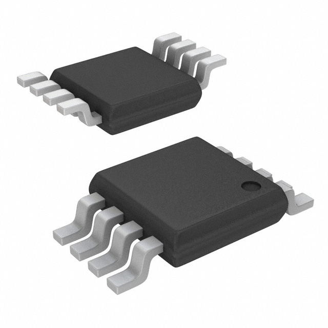
product image

LTC6416 Picture
SeekIC No. : 004402670 Detail

LTC6416: Features: 2GHz 3dB Small Signal Bandwidth 300MHz ±0.1dB Bandwidth 1.8nV/Hz Output Noise46.25dBm Equivalent OIP3 at 140MHz 40.25dBm Equivalent OIP3 Up to 300MHz81dBc/72dBc HD2/HD3 at 140MHz, 2VP-P O...

floor Price/Ceiling Price

Part Number:
LTC6416
Supply Ability:
5000

Price Break

  • Qty
  • 1~5000
  • Unit Price
  • Negotiable
  • Processing time
  • 15 Days
Total Cost: $ 0.00

SeekIC Buyer Protection PLUS - newly updated for 2013!

  • Escrow Protection.
  • Guaranteed refunds.
  • Secure payments.
  • Learn more >>

Month Sales

268 Transactions

Rating

evaluate  (4.8 stars)

Upload time: 2025/2/15

Payment Methods

All payment methods are secure and covered by SeekIC Buyer Protection PLUS.

Notice: When you place an order, your payment is made to SeekIC and not to your seller. SeekIC only pays the seller after confirming you have received your order. We will also never share your payment details with your seller.
Product Details

Description


Features:

2GHz 3dB Small Signal Bandwidth
300MHz ±0.1dB Bandwidth
1.8nV/Hz Output Noise
46.25dBm Equivalent OIP3 at 140MHz
40.25dBm Equivalent OIP3 Up to 300MHz
81dBc/72dBc HD2/HD3 at 140MHz, 2VP-P Out
84.5dBc IM3 at 140MHz, 2VP-P Out Composite
74dBc/67.5dBc HD2/HD3 at 300MHz, 2VP-P Out
72.5dBc IM3 at 300MHz, 2VP-P Out Composite
Programmable High Speed, Fast Recovery Output Clamping
DC-Coupled Signal Path
Operates on Single 2.7V to 3.9V Supply
Low Power: 150mW on 3.6V
2mm * 3mm 10-Pin DFN Package


Application

  Differential ADC Driver
  IF Sampling Receivers
 Impedance Transformer
  SAW Filter Interface
 CCD Buffer


Pinout

  Connection Diagram


Specifications

Total Supply Voltage (V+ to GND)................................4V
Input Current (CLLO, CLHI, VCM, IN+, IN) ...........±10mA
Output Current (OUT+, OUT) ...........................±22.5mA
Operating Temperature Range (Note 2)....40 to 85
Specifi ed Temperature Range (Note 3) ....40 to 85
Storage Temperature Range ...................65to 150
Junction Temperature ........................................... 150


Description

The LTC®6416 is a differential unity gain buffer designed to drive 16-bit ADCs with extremely low output noise and excellent linearity beyond 300MHz. Differential input impedance is 12k, allowing 1:4 and 1:8 transformers to be used at the input to achieve additional system gain.

With no external biasing or gain setting components and a fl ow-through pinout, the LTC6416 is very easy to use.

It can be DC-coupled and has a common mode output offset of 40mV. If the input signals are AC-coupled, the LTC6416 input pins are internally biased to provide an output common mode voltage that is set by the voltage on the VCM pin.

In addition the LTC6416 has high speed, fast recovery clamping circuitry to limit output signal swing. Both the high and low clamp voltages are internally biased to allow maximum output swing but are also user programmable via the CLLO and CLHI pins.

Supply current is nominally 42mA and the LTC6416 operates on supply voltages ranging from 2.7V to 3.9V.
The LTC6416 is packaged in a 10-lead 3mm * 2mm DFN package. Pinout is optimized for placement directly adjacent to Linear's high speed 12-, 14- and 16-bit ADCs.


Customers Who Bought This Item Also Bought

Margin,quality,low-cost products with low minimum orders. Secure your online payments with SeekIC Buyer Protection.
Crystals and Oscillators
Inductors, Coils, Chokes
Circuit Protection
Cable Assemblies
Transformers
Sensors, Transducers
View more