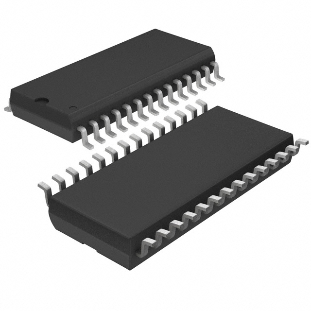
Features: SpecificationsDescriptionThe LTC4403-1 is designed as multiband RF power controllers for EDGE/TDMA. It has two outputs to control dual TX PA modules with two control inputs. An internal sample and hold circuit enables it to be used with AM modulation via the carrier or PA supply. The inp...
LTC4403-1: Features: SpecificationsDescriptionThe LTC4403-1 is designed as multiband RF power controllers for EDGE/TDMA. It has two outputs to control dual TX PA modules with two control inputs. An internal sa...
SeekIC Buyer Protection PLUS - newly updated for 2013!
268 Transactions
All payment methods are secure and covered by SeekIC Buyer Protection PLUS.
The LTC4403-1 is designed as multiband RF power controllers for EDGE/TDMA. It has two outputs to control dual TX PA modules with two control inputs. An internal sample and hold circuit enables it to be used with AM modulation via the carrier or PA supply. The input voltage range is optimized for operation from a single lithium-ion cell or 3 x NiMH.
LTC4403-1 has many features. The first one is supports AM modulation in EDGE/TDMA (ANSI-136) applications. The second one is single output RF power amplifier control. The third one is internal schottky diode detector with >40dB range. The fourth one is wide input frequency range which would be from 800MHz to 2.4GHz. The fifth one is autozero loop cancels offset errors and
temperature dependent offsets. The sixth one is wide VIN range from 2.7V to 6V. The seventh one is allows direct connection to battery. The eighth one is RF output power set by external DAC. The ninth one is internal frequency compensation. The tenth one is rail-to-rail power control outputs. The eleventh one is low operating current which would be 1mA. The twelfth one is low shutdown current which would be less than 10mA. The thirteenth one is PCTL input filter. The fourteenth one is available in a 8-Pin MSOP package. That are all the main features.
Some absolute maximum ratings of LTC4403-1 have been concluded into several points as follow. The first one is about its VIN to GND which would be from -0.3V to 6.5V. The second one is about its VPCA, VPCB voltage which would be from -0.3V to 4.6V. The third one is about its PCTL voltage which would be from -0.3V to (VIN + 0.3V). The fourth one is about its RF voltage which would be (VIN ± 2.6V) to 7V. The fifth one is about its SHDN, VHOLD, BSEL voltage to GND which would be from -0.3V to (VIN + 0.3V). And so on. For more information please contact us.