LTC4301LCDD8

Features: Level Translates 1V Signals to Standard 3.3V and 5V Logic Rails Allows Bus Pull-Up Voltages as Low as 1V on SDAIN and SCLIN Bidirectional Buffer* for SDA and SCL Lines Increases Fanout Prevents SDA and SCL Corruption During Live Board Insertion and Removal from Backplane Isolates Input ...

product image

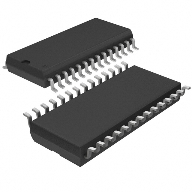
LTC4301LCDD8 Picture
SeekIC No. : 004402556 Detail

LTC4301LCDD8: Features: Level Translates 1V Signals to Standard 3.3V and 5V Logic Rails Allows Bus Pull-Up Voltages as Low as 1V on SDAIN and SCLIN Bidirectional Buffer* for SDA and SCL Lines Increases Fanout Pr...

floor Price/Ceiling Price

Part Number:
LTC4301LCDD8
Supply Ability:
5000

Price Break

  • Qty
  • 1~5000
  • Unit Price
  • Negotiable
  • Processing time
  • 15 Days
Total Cost: $ 0.00

SeekIC Buyer Protection PLUS - newly updated for 2013!

  • Escrow Protection.
  • Guaranteed refunds.
  • Secure payments.
  • Learn more >>

Month Sales

268 Transactions

Rating

evaluate  (4.8 stars)

Upload time: 2024/12/21

Payment Methods

All payment methods are secure and covered by SeekIC Buyer Protection PLUS.

Notice: When you place an order, your payment is made to SeekIC and not to your seller. SeekIC only pays the seller after confirming you have received your order. We will also never share your payment details with your seller.
Product Details

Description


Features:

Level Translates 1V Signals to Standard 3.3V and 5V Logic Rails
Allows Bus Pull-Up Voltages as Low as 1V on SDAIN and SCLIN
Bidirectional Buffer* for SDA and SCL Lines Increases Fanout
Prevents SDA and SCL Corruption During Live Board Insertion and Removal from Backplane
Isolates Input SDA and SCL Line from Output
10kV Human Body Model ESD Protection
Supports Clock Stretching, Arbitration and Synchronization
High Impedance SDA, SCL Pins for VCC = 0V
CS Gates Connection from Input to Output
Compatible with I2CTM, I2C Fast Mode and SMBus Standards (Up to 400kHz Operation)
Small 8-Pin MSOP and DFN (3mm*3mm) Packages


Application

Hot Board Insertion
Servers
Capacitance Buffer/Bus Extender
Desktop Computers


Pinout

  Connection Diagram


Specifications

VCC to GND ................................................. 0.3V to 7V
SDAIN, SCLIN, SDAOUT, SCLOUT, CS .......... 0.3V to 7V
READY ......................................................... 0.3V to 6V
Operating Temperature Range
    LTC4301LC ............................................. 0°C to 70°C
    LTC4301LI............................................... 40°C to 85°C
Storage Temperature Range
   MSOP ....................................................... 65°C to 150°C
   DFN ......................................................... 65°C to 125°C
Lead Temperature (Soldering, 10 sec)........ 300°C


Description

The LTC4301LCDD8 hot swappable, 2-wire bus buffer allows I/O card insertion into a live backplane without corruption of the data and clock busses. In addition, the LTC4301LCDD8 SDAIN and SCLIN pins are compatible with systems with pull-up voltages as low as 1V. Control circuitry prevents the backplane from being connected to the card until a stop bit or a bus idle is present. When the connection is made, the LTC4301LCDD8 provides bidirectional buffering, keeping the backplane and card capacitances isolated.

When driven low, the CS input pin of LTC4301LCDD8 allows the part to connect after a stop bit or bus idle occurs. Driving CS high breaks the connection between SCLIN and SCLOUT and between SDAIN and SDAOUT. A logic high on READY indicates that the backplane and card sides are connected together.

The LTC4301LCDD8 is offered in 8-pin DFN (3mm ×3mm) and MSOP packages


Customers Who Bought This Item Also Bought

Margin,quality,low-cost products with low minimum orders. Secure your online payments with SeekIC Buyer Protection.
Soldering, Desoldering, Rework Products
Potentiometers, Variable Resistors
Prototyping Products
DE1
Crystals and Oscillators
Circuit Protection
View more