LTC3831-1

Features: · VOUT as Low as 0.4V· High Power Switching Regulator Controller for DDR Memory Termination· VOUT Tracks 1/2 of VIN or External VREF· No Current Sense Resistor Required· Low VCC Supply: 3V to 8V· Maximum Duty Cycle > 91% Over Temperature· Drives All N-Channel External MOSFETs· High Ef...

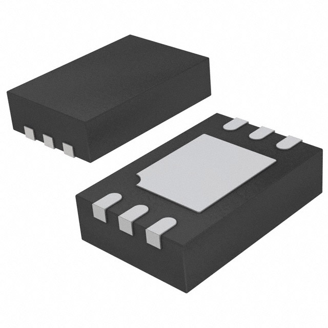
product image

LTC3831-1 Picture
SeekIC No. : 004402380 Detail

LTC3831-1: Features: · VOUT as Low as 0.4V· High Power Switching Regulator Controller for DDR Memory Termination· VOUT Tracks 1/2 of VIN or External VREF· No Current Sense Resistor Required· Low VCC Supply: 3V...

floor Price/Ceiling Price

Part Number:
LTC3831-1
Supply Ability:
5000

Price Break

  • Qty
  • 1~5000
  • Unit Price
  • Negotiable
  • Processing time
  • 15 Days
Total Cost: $ 0.00

SeekIC Buyer Protection PLUS - newly updated for 2013!

  • Escrow Protection.
  • Guaranteed refunds.
  • Secure payments.
  • Learn more >>

Month Sales

268 Transactions

Rating

evaluate  (4.8 stars)

Upload time: 2024/11/24

Payment Methods

All payment methods are secure and covered by SeekIC Buyer Protection PLUS.

Notice: When you place an order, your payment is made to SeekIC and not to your seller. SeekIC only pays the seller after confirming you have received your order. We will also never share your payment details with your seller.
Product Details

Description


Features:

· VOUT as Low as 0.4V
· High Power Switching Regulator Controller for DDR Memory Termination
· VOUT Tracks 1/2 of VIN or External VREF
· No Current Sense Resistor Required
· Low VCC Supply: 3V to 8V
· Maximum Duty Cycle > 91% Over Temperature
· Drives All N-Channel External MOSFETs
· High Efficiency: Up to 95%
· Programmable Fixed Frequency Operation: 100kHz to 500kHz
· External Clock Synchronization Operation
· Programmable Soft-Start
· Low Shutdown Current: <10mA
· Overtemperature Protection
· Available in 16-Pin Narrow SSOP Package


Application

· DDR SDRAM Termination
· SSTL_2, SSTL_3 Interface
· HSTL Interface


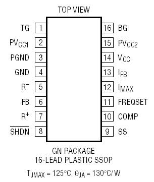
Pinout

  Connection Diagram


Specifications

Supply Voltage
VCC ............................................................................... 9V
PVCC1,2 .......................................................................14V
Input Voltage
IFB, IMAX ......................................................0.3V to 14V
R+, R, FB, SHDN, FREQSET ............. 0.3V to VCC + 0.3V
Junction Temperature (Note 9) .............................. 125°C
Operating Temperature Range (Note 4) ..40°C to 85°C
Storage Temperature Range ............. .. 65°C to 150°C
Lead Temperature (Soldering, 10 sec).................... 300°C


Description

The LTC®3831-1 is a high power, high efficiency switching regulator controller designed for DDR memory termination. The LTC3831-1 generates an output voltage equal to 1/2 of an external supply or reference voltage. The LTC3831-1 uses a synchronous switching architecture with N-channel MOSFETs. Additionally, the chip senses output current through the drain-source resistance of the upper N-channel FET, providing an adjustable current limit without a current sense resistor.

The LTC3831-1 operates with input supply voltage as low as 3V and with a maximum duty cycle of >91%. It includes a fixed frequency PWM oscillator for low output ripple operation. The 300kHz free-running clock frequency can be externally adjusted or synchronized with an external signal from 100kHz to above 500kHz. In shutdown mode, the device supply current drops to <10mA.


Customers Who Bought This Item Also Bought

Margin,quality,low-cost products with low minimum orders. Secure your online payments with SeekIC Buyer Protection.
Soldering, Desoldering, Rework Products
Crystals and Oscillators
Discrete Semiconductor Products
RF and RFID
Transformers
Circuit Protection
View more