Features: · Very Low VIN(MIN): 1.5V
· Ultrafast Transient Response
· True Current Mode Control
· 5V Drive for N-Channel MOSFETs Eliminates Auxillary 5V Supply
· No Sense Resistor Required
· Uses Standard 5V Logic-Level N-Channel MOSFETs
· VOUT(MIN): 0.4V
· VOUT Tracks 1/2 VIN or External VREF
· Symmetrical Source and Sink Output Current Limit
· Adjustable Switching Frequency
· tON(MIN) <100ns
· Power Good Output Voltage Monitor
· Programmable Soft-Start
· Output Overvoltage Protection
· Optional Short-Circuit Shutdown Timer
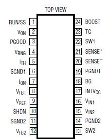
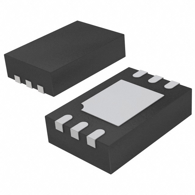
· Small 24-Lead SSOP Package
Application· Bus Termination: DDR/QDR Memory, SSTL, HSTL, ...
· Servers, RAID Systems
· Distributed Power Systems
· Synchronous Buck with General Purpose Boost
Pinout Specifications
Input Supply Voltage (VIN2) ..................10V to 0.3V
Boosted Topside Driver Supply Voltage
(BOOST) ............................................... 42V to 0.3V
VIN1, ION, SW1 Voltage ......................... 36V to 0.3V
RUN/SS, PGOOD Voltages ....................... 7V to 0.3V
VON, VREF, VRNG Voltages ....(INTVCC + 0.3V) to 0.3V
ITH, VFB1 Voltages ................................ 2.7V to 0.3V
SW2 Voltage ......................................... 36V to 0.4V
VFB2 Voltage .............................................VIN2 + 0.3V
SHDN Voltage ....................................................... 10V
TG, BG, INTVCC Peak Currents................................ 2A
TG, BG, INTVCC RMS Currents ............................ 50mA
Operating Ambient Temperature
Range (Note 4) ................................ 40°C to 85°C
Junction Temperature (Note 2) ....................... 125°C
Storage Temperature Range ......... 65°C to 150°C
Lead Temperature (Soldering, 10 sec)............. 300°C
DescriptionThe LTC®3718 is a high current, high efficiency synchronous switching regulator controller for DDR and QDRTM memory termination. It operates from an input as low as 1.5V and provides a regulated output voltage equal to (0.5)VIN. The controller uses a valley current control architecture to enable high frequency operation with very low on-times without requiring a sense resistor. Operating frequency is selected by an external resistor and is compensated for variations in VIN and VOUT. The LTC3718 uses a pair of standard 5V logic level N-channel external MOSFETs, eliminating the need for expensive P-channel or low threshold devices.
Forced continuous operation of LTC3718 reduces noise and RF interference. Fault protection is provided by internal foldback current limiting, an output overvoltage comparator and anoptional short-circuit timer. Soft-start capability for supply sequencing can be accomplished using an externaltiming capacitor. OPTI-LOOP® compensation allows thetran sient response to be optimized over a wide range of loads and output capacitors.

 LTC3718 Data Sheet


